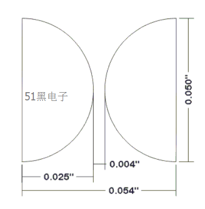
有时为了降低成本,利用铜皮做ESD防护,铜皮的制作。可以参考
An excellent way that I have found to protect inputs to electronics components from the very high
voltages of ESD and EMI spikes is to use spark gaps. These can be built into your circuit board as
a part of the PC board etch. The gaps should be designed as shown in the following dimension
drawing.

As shown above the two spark gap pads are half circles with a radius of 0.025 inches. The
designed gap spacing should be 0.004 inches. If you use care in the manufacturing process so that
the board's final etched gap dimension is less than 0.005 to 0.006 inches then you can expect to
have an air gap that can clamp ESD spikes to less than 200 volts. The gap area MUST be open to
the air and NOT covered with solder mask.
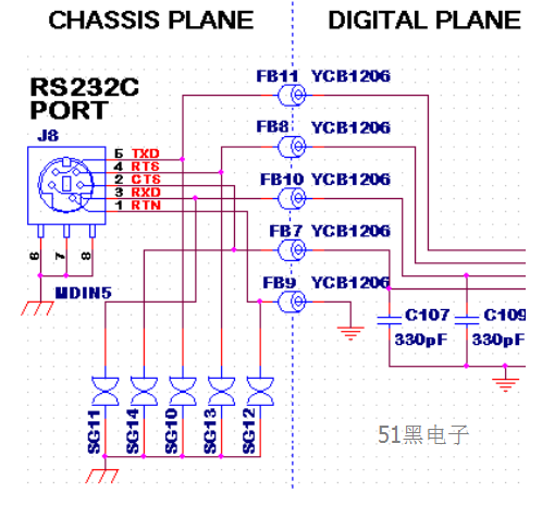
The spark gap can be a very effective protection measure, particularly if used in conjunction with
other filtering components. The schematic snippett below shows how the spark gaps can be drawn
directly onto the schematic as an actual "component".

完整的pdf格式文档51黑下载地址:
 焊盘间隙放电Spark Gaps.pdf
(1.58 MB, 下载次数: 41)
|