|
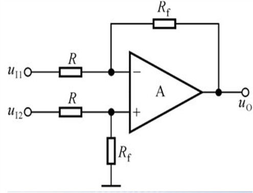
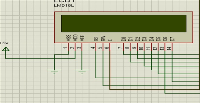
基于TMS320F28027芯片的微弱电压信号测量,熟练掌握DSP开发环境CCS软件以及Proteus电路设计软件,掌握微弱电压的测量方式,掌握TMS320F28027芯片的基本IO操作、中断方式、ADC功能的使用,进一步了解DSP系统的特点。 基于TMS320F28027芯片的微弱电压信号测量方案包括如下几部分: 为了便于对微弱电压(2*(10-3)*sin(100pi*t))进行测量,设计运算放大电路对微弱电压进行放大处理,使得电压变为0~3.2V,电路设计如下: 电压计算公式:Vout=Rf/R*(u11-u12); (2)基于TMS320F28027的电压信号采集及转换 TMS320F28027的ADC功能: 1.12位双采样保持电路。 2.同时采样和序列采样方式。 3.全范围电压输入,0V到3.3V固定,或者VREFLO到VREFHI可调。 4.系统时钟全频运行,无需分频。 5.16输入通道。 6.16个SOC配置,设置触发,采样窗口,通道。 7.16个独立保存转换结果的结果寄存器。 8.多触发源。 9.9个灵活的PIE中断 ADC采集电压计算公式如下: Vol=(AdcResult.ADCRESULT0)/4096*3.3; (3)电压的动态显示 测量到电压后进行显示,本次实验采用LM016L型号LCD显示器进行电压显示。 引脚接口说明: 第1脚:VSS为地电源。 第2脚:VDD接5V正电源。 第3脚:VL为液晶显示器对比度调整端,接正电源时对比度最弱,接地时对比度最高。 第4脚:RS为寄存器选择,高电平时选择数据寄存器、低电平时选择指令寄存器。 第5脚:R/W为读写信号线,高电平时进行读操作,低电平时进行写操作。当RS和R/W共同为低电平时可以写入指令或者显示地址,当RS为低电平R/W为高电平时可以读忙信号,当RS为高电平R/W为低电平时可以写入数据。 第6脚:E端为使能端,当E端由高电平跳变成低电平时,液晶模块执行命令。 第7~14脚:D0~D7为8位双向数据线。 LM016L接线如下所示: 指令如下所示:
芯片时序表如下: | | | | | | | RS=L,R/W=L,D0—D7=指令码,E=高脉冲 | | | | | | | | | | RS=H,R/W=L,D0—D7=数据,E=高脉冲 | | |
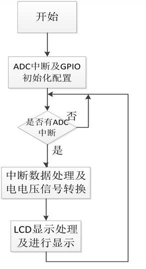
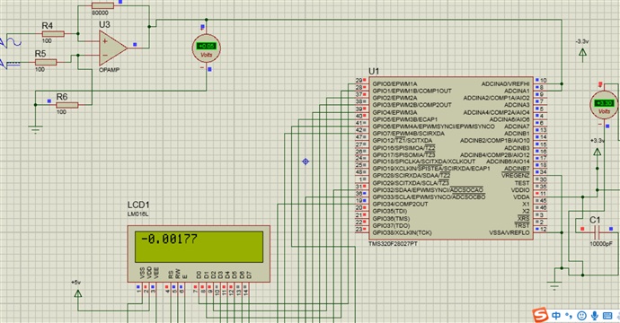
(2)程序流程图 电路设计如下: 程序如下所示: 在Proteus软件进行仿真,仿真结果截图如下: LCD显示小数点后5位,输入正弦电压幅值为0.002,显示精度为百分之一。
全部资料51hei下载地址: | 


 [复制链接]


 QQ好友和群
 QQ空间
QQ空间 腾讯微博
腾讯微博 腾讯朋友
腾讯朋友 收藏
收藏 淘帖
淘帖 顶
顶 踩
踩 谢谢楼主
谢谢楼主