1. 引言
20世纪末,电子技术获得了飞速的发展,在其推动下,现代电子产品几乎渗透了社会的各个领域,有力地推动了社会生产力的发展和社会信息化程度的提高,同时也使现代电子产品性能进一步提高,产品更新换代的节奏也越来越快。
时间对人们来说总是那么宝贵,工作的忙碌性和繁杂性容易使人忘记当前的时间。忘记了要做的事情,当事情不是很重要的时候,这种遗忘无伤大雅。但是,一旦重要事情,一时的耽误可能酿成大祸。例如,许多火灾都是由于人们一时忘记了关闭煤气或是忘记充电时间。尤其在医院,每次护士都会给病人作皮试,测试病人是否对药物过敏。注射后,一般等待5分钟,一旦超时,所作的皮试试验就会无效。手表当然是一个好的选择,但是,随着接受皮试的人数增加,到底是哪个人的皮试到时间却难以判断。所以,要制作一个定时系统。随时提醒这些容易忘记时间的人。
钟表的数字化给人们生产生活带来了极大的方便,而且大大地扩展了钟表原先的报时功能。诸如定时自动报警、按时自动打铃、时间程序自动控制、定时广播、定时启闭电路、定时开关烘箱、通断动力设备,甚至各种定时电气的自动启用等,所有这些,都是以钟表数字化为基础的。因此,研究数字钟及扩大其应用,有着非常现实的意义。
基于单片机的定时和控制装置在许多行业有着广泛的应用,数字钟作为其中最基本的一个应用实例,具有结构简单应用广泛的特点。数字钟中使用了单片机中最为常用的输入输出设备按键开关和数码管;数字钟程序主要应用单片机的定时器和中断实现计时和显示功能。当今数字种作为一个单元电路被广泛应用于电子表、电子万年历等产品中,带来广泛的经济效益。
目前的单片机产品普遍要求体积小、重量轻,这就要求单片机除了功能强和功耗低外,还要求其体积要小。现在虽然单片机的品种繁多,各具特色,但仍以80C51为核心的单片机占主流,兼容其结构和指令系统的有PHILIPS公司的产品,ATMEL公司的产品和Winbond系列单片机。所以C8051为核心的单片机占据了半壁江山。而Microchip公司的PIC精简指令集(RISC)也有着强劲的发展势头,HOLTEK公司近年的单片机产量与日俱增,与其低价质优的优势,占据一定的市场分额。此外还有MOTOROLA公司的产品,日本几大公司的专用单片机。在一定的时期内,这种情形将得以延续,将不存在某个单片机一统天下的垄断局面,走的是依存互补,相辅相成、共同发展的道路。单片机的可靠性及应用水平越来越高和互联网连接已是一种明显的走向。单片机从功能上讲可以说是万用机。目前,单片机正朝着高性能和多品种方向发展,趋势将是进一步向着CMOS化、低功耗、小体积、大容量、高性能、低价格和外围电路内装化等几个方面发展。当今,单片机广泛地用于各种仪器仪表,使仪器仪表智能化,并可以提高测量的自动化程度和精度,简化仪器仪表的硬件结构,提高其性能价格比。单片机也广泛地用于各种实时控制系统中。例如,在工业测控、航空航天、尖端武器、机器人等各种实时控制系统中,都可以用单片机作为控制器。单片机的实时数据处理能力和控制功能,可使系统保持在最佳工作状态,提高系统的工作效率和产品质量。自从单片机诞生以后,它就步入了人类生活,如洗衣机、电冰箱、电子玩具、收录机等家用电器配上单片机后,提高了智能化程度,增加了功能,倍受人们喜爱。单片机将使人类生活更加方便、舒适、丰富多彩。单片机已成为计算机发展和应用的一个重要方面。单片机应用的重要意义还在于,它从根本上改变了传统的控制系统设计思想和设计方法。从前必须由模拟电路或数字电路实现的大部分功能,现在已能用单片机通过软件方法来实现了。这种软件代替硬件的控制技术也称为微控制技术,是传统控制技术的一次革命。随着半导体工艺技术的发展及系统设计水平的提高,单片机还会不断产生新的变化和进步。在不久的将来,最终单片机与微机系统之间的距离越来越小,甚至难以辨认。
2.关于单片机
2.1单片机的发展
单片机自问世以来,性能不断提高和完善,其资源又能满足很多应用场合的需要,加之单片机具有集成度高、功能强、速度快、体积小、功耗低、使用方便、价格低廉等特点,因此,在工业控制、智能仪器仪表、数据采集和处理、通信系统、高级计算器、家用电器等领域的应用日益广泛,并且正在逐步取代现有的多片微机应用系统。单片机的潜力越来越被人们所重视。特别是当前用CMOS工艺制成的各种单片机,由于功耗低,使用的温度范围大,抗干扰能力强、能满足一些特殊要求的应用场合,更加扩大了单片机的应用范围,也进一步促使单片机性能的发展。而现在单片机在液晶显示上也有了很多的应用。
随着科技不断进步,各种显示技术如雨后春笋般诞生,由于液晶显示器(LCD)具有轻薄短小、低耗电量、无辐射危险,平面直角显示以及影像稳定不闪烁等优势,在近年来价格不断下跌的吸引下,逐渐取代CRT之主流地位,显示器明日之星架势十足。液晶显示器件从初期的实验室到现在的生产厂家,已形成较大规模的生产能力,使液晶显示形成了独立的产业部门。而今,液晶显示已经应用于人们生产、生活中的各个领域,人们时时处处都要与这一神奇而又普通的产品打交道。液晶显示技术以它跨越多学科的工作原理,高技术、专业化的制造工艺使它披上了一层神秘的面纱,而它轻巧薄形的体态,独特而理想的性能以及广泛的应用价值,又使它充满魅力,深深地吸引着人们。
在单片机技术日趋成熟的今天,其灵活的硬件电路的设计和软件的设计,让单片机得到了广泛的应用,几乎是从小的电子产品,到大的工业控制,单片机都起到了举足轻重的作用。单片机小的系统结构几乎是所有具有可编程硬件的一个缩影,可谓是“麻雀虽小,肝胆俱全”,单片机的学习和研究是对微机系统学习和研究的简捷途径。
在目前,用户对单片机的需要越来越多,但是,要求也越来越高,因此,单片机也在不断的发展和进步。单片机的技术进步主要反映在内部结构、功率消耗、外部电压等级以及制造工艺上。在这几方面,较为典型地说明了数字单片机的水平。下面分别就这三个方面说明单片机的技术进步状况。
(1)内部结构的进步
单片机在内部已集成了越来越多的部件,这些部件包括一般常用的电路,例如:定时器,比较器,A/转换器,D /A转换器,串行通信接口,Watchdog电路,LCD控制器等。
有的单片机为了构成控制网络或形成局部网,内部含有局部网络控制模块CAN。例如,Infineon公司的C 505C,C515C,C167CR,C167CS-32FM,81C90;Motorola公司的68HC08AZ 系列等。特别是在单片机C167CS-32FM中,内部还含有2个CAN。因此,这类单片机十分容易构成网络。特别是在控制,系统较为复杂时,构成一个控制网络十分有用。
为了能在变频控制中方便使用单片机,形成最具经济效益的嵌入式控制系统。有的单片机内部设置了专门用于变频控制的脉宽调制控制电路,这些单片机有Fujitsu公司的MB89850系列、MB89860系列;Motorola 公司的MC68HC08MR16、MR24等。在这些单片机中,脉宽调制电路有6个通道输出,可产生三相脉宽调制交流电压,并内部含死区控制等功能。
(2)功耗、封装及电源电压的进步
现在新的单片机的功耗越来越小,特别是很多单片机都设置了多种工作方式,这些工作方式包括等待,暂停,睡眠,空闲,节电等工作方式。Philips公司的单片机P87LPC762是一个很典型的例子,在空闲时,其功耗为1.5 mA,而在节电方式中,其功耗只有0.5mA。而在功耗上最令人惊叹的是TI公司的单片机MSP430系列,它是一个 16位的系列,有超低功耗工作方式。它的低功耗方式有LPM1、LPM3、LPM4三种。当电源为3V时,如果工作于 LMP1方式,即使外围电路处于活动,由于CPU不活动,振荡器处于1~4MHz,这时功耗只有50?A。在LPM3 时,振荡器处于32kHz,这时功耗只有1.3?A。在LPM4时,CPU、外围及振荡器32kHz都不活动,则功耗只有0.1?A。
现在单片机的封装水平已大大提高,随着贴片工艺的出现,单片机也大量采用了各种合符贴片工艺的封装方式出现,以大量减少体积。在这种形势中,Microchip公司推出的8引脚的单片机特别引人注目。这是PIC12CXXX系列。它含有0.5~2K程序存储器,25~128字节数据存储器,6个I/O端口以及一个定时器,有的还含4道A/D ,完全可以满足一些低档系统的应用。扩大电源电压范围以及在较低电压下仍然能工作是今天单片机发展的目标之一。目前,一般单片机都可以在3.3~5.5V的条件下工作。而一些厂家,则生产出可以在2.2~6V的条件下工作的单片机。这些单片机有Fujitsu公司的MB89191~89195,MB89121~125A,MB89130系列等,应该说该公司的F2MC-8L系列单片机绝大多数都满足2.2~6V的工作电压条件。而TI公司的MSP430X11X系列的工作电压也是低达2.2V的。
(3)工艺上的进步
现在的单片机基本上采用CMOS技术,但已经大多数采用了0.6?m以上的光刻工艺,有个别的公司,如Motorola公司则已采用0.35?m甚至是0.25?m技术。这些技术的进步大大地提高了单片机的内部密度和可靠性。
单片机在目前的发展形势下,可靠性及应用越来越高的水平和互联网连接已是一种明显的走向。所集成的部件越来越多;NS(美国国家半导体)公司的单片机已把语音、图象部件也集成到单片机中,也就是说,单片机的意义只是在于单片集成电路,而不在于其功能了;如果从功能上讲它可以讲是万用机。原因是其内部已集成上各种应用电路。 功耗越来越低和模拟电路结合越来越多也将会成为单片机的一个发展的方向。随着半导体工艺技术的发展及系统设计水平的提高,单片机还会不断产生新的变化和进步,最终人们可能发现:单片机与微机系统之间的距离越来越小,甚至难以辨认。
2.2 单片机的开发背景
现代工业控制和一些智能化仪器仪表中,越来越多的场所需要用点阵图形显示器显示汉字。液晶显示器是人与机器沟通的重要界面,而且液晶显示器也有如下特点,开发出来会有很大的应用空间。液晶显示器目前发展最快,也已经成为电子信息产业的支柱性产业之一,受到普遍关注与重视。那么液晶显示器与传统的显示器相比,到底有什么新的特点呢?
⑴ 质量高 由于液晶显示器每一个点在收到信号后就一直保持那种色彩和亮度,恒定发光,而不像阴极射线管显示器(CRT)那样需要不断刷新亮点。因此,液晶显示器画质高而且绝对不会闪烁,把眼睛疲劳降到最低。
⑵ 没有电磁辐射 传统显示器的显示材料是荧光粉,通过电子束撞击荧光粉而显示,电子束在打到荧光粉上的一刹那间会产生强大的电磁辐射,尽管目前有许多显示器产品在处理辐射问题上进行了比较有效的处理,尽可能地把辐射量降到最低,但要彻底消除是困难的。相对来说,液晶显示器在防止辐射方面具有先天的优势,因为它根本就不存在辐射。
⑶ 可视面积大 对于相同尺寸的显示器来说,液晶显示器的可视面积要更大一些。液晶显示器的可视面积跟它的对角线尺寸相同。阴极射线管显示器显像管前面板四周有一英寸左右的边框不能用于显示。
⑷ 应用范围广 最初的液晶显示器由于无法显示细腻的字符,通常应用在电子表、计算器上。而随后出现的DSTN和TFT则被广泛制作成电脑中的液晶显示设备,DSTN液晶显示屏用于早期的笔记本电脑;TFT则既应用在笔记本电脑上(现在大多数笔记本电脑都使用TFT显示屏),又用于主流台式显示器上。
⑸ 画面效果好 与传统显示器相比,液晶显示器一开始就使用纯平面的玻璃板,其显示效果是平面直角的,让人有一种耳目一新的感觉。而且液晶显示器更容易在小面积屏幕上实现高分辨率。
⑹ 数字式接口 液晶显示器都是数字式的,不像阴极射线管彩显采用模拟接口。也就是说,使用液晶显示器,显卡再也不需要像往常那样把数字信号转化成模拟信号再行输出了。理论上,这会使色彩和定位都更加准确完美。
⑺ 体积小 传统的阴极射线管显示器,后面总是拖着一个笨重的射线管。液晶显示器突破了这一限制,给人一种全新的感觉。传统显示器是通过电子枪发射电子束到屏幕,因而显像管的管颈不能做得很短,当屏幕增加时也必然增大整个显示器的体积。而液晶显示器通过显示屏上的电极控制液晶分子状态来达到显示目的,即使屏幕加大,它的体积也不会成正比的增加,而且在重量上比相同显示面积的传统显示器要轻得多。
⑻ 功率消耗小 传统的显示器内部由许多电路组成,这些电路驱动着阴极射线显像管工作时,需要消耗很大的功率,而且随着体积的不断增大,其内部电路消耗的功率肯定也会随之增大。相比而言,液晶显示器的功耗主要消耗在其内部的电极和驱动IC上,因而耗电量比传统显示器也要小得多。
2.3 AT89S52单片机
AT89S52 是一种低功耗、高性能CMOS8 位微控制器,具有8K 在系统可编程存储器。使用Atmel 公司高密度非易失性存储器技术制造,与工业80C51产品指令和引脚完全兼容。片上Flash 允许程序存储器在系统可编程,亦适于常规编程器。在单芯片上,拥有灵巧的8 位CPU 和在系统可编程Flash ,使得AT89S52 为众多嵌入式控制应用系统提供高灵活、超有效的解决方案。AT89S52 具有以下标准功能:8k 字节Flash,256 字节RAM,32 位I/O 口线,看门狗定时器,2 个数据指针,三个16 位定时器/计数器,一个6 向量2 级中断结构,全双工串行口,片内晶振及时钟电路。另外,AT89S52 可降至0Hz 静态逻辑操作,支持2 种软件可选择节电模式。空闲模式下,CPU停止工作,允许RAM 、定时器/计数器、串口、中断继续工作。掉电保护方式下,RAM 内容被保存,振荡器被冻结,单片机一切工作停止,直到下一个中断或硬件复位为止。
 图2-1AT89S52的引脚
2.3.1 AT89S52单片机引脚功能
P0 口:P0 口是一个8 位漏极开路的双向I/O 口。作为输出口,每位能驱动8 个TTL 逻辑电平。对P0 端口写“1”时,引脚用作高阻抗输入。当访问外部程序和数据存储器时,P0 口也被作为低8 位地址/数据复用。在这种模式下,P0 具有内部上拉电阻。
P1 口:P1 口是一个具有内部上拉电阻的8 位双向I/O 口,P1 输出缓冲器能驱动4 个TTL 逻辑电平。对P1 端口写“1”时,内部上拉电阻把端口拉高,此时可以作为输入口使用。作为输入使用时,被外部拉低的引脚由于内部电阻的原因,将输出电流(IIL)。此外,P1.0 和P1.2 分别作定时器/计数器2 的外部计数输入(P1.0/T2)和时器/计数器2的触发输入(P1.1/T2EX),具体如下表所示。在flash 编程和校验时,P1 口接收低8 位地址字节。
P2 口:P2 口是一个具有内部上拉电阻的8 位双向I/O 口,P2 输出缓冲器能驱动4 个TTL 逻辑电平。对P2 端口写“1”时,内部上拉电阻把端口拉高,此时可以作为输入口使用。作为输入使用时,被外部拉低的引脚由于内部电阻的原因,将输出电流(IIL)。在访问外部程序存储器或用16 位地址读取外部数据存储器(例如执行MOVX @DPTR)时,P2 口送出高八位地址。在这种应用中,P2 口使用很强的内部上拉发送1。在使用8 位地址(如MOVX @RI )访问外部数据存储器时,P2 口输出P2 锁存器的内容。
P3 口:P3 口是一个具有内部上拉电阻的8 位双向I/O 口,p2 输出缓冲器能驱动4 个TTL 逻辑电平。对P3 端口写“1”时,内部上拉电阻把端口拉高,此时可以作为输入口使用。作为输入使用时,被外部拉低的引脚由于内部电阻的原因,将输出电流(IIL)。
RST: 复位输入。晶振工作时,RST 脚持续2 个机器周期高电平将使单片机复位。看门狗计时完成后,RST 脚输出96 个晶振周期的高电平。特殊寄存器AUXR( 地址8EH) 上的DISRTO 位可以使此功能无效。DISRTO 默认状态下,复位高电平有效。
ALE/PROG:地址锁存控制信号(ALE)是访问外部程序存储器时,锁存低8 位地址的输出脉冲。在flash 编程时,此引脚(PROG )也用作编程输入脉冲。在一般情况下,ALE 以晶振六分之一的固定频率输出脉冲,可用来作为外部定时器或时钟使用。然而,特别强调,在每次访问外部数据存储器时,ALE 脉冲将会跳过。如果需要,通过将地址为8EH 的SFR 的第0 位置“1”,ALE 操作将无效。这一位置“1”,ALE 仅在执行MOVX 或MOVC 指令时有效。
PSEN: 外部程序存储器选通信号(PSEN)是外部程序存储器选通信号。当AT89S52 从外部程序存储器执行外部代码时,PSEN 在每个机器周期被激活两次,而在访问外部数据存储器时,PSEN 将不被激活。
EA/VPP: 访问外部程序存储器控制信号。为使能从0000H 到FFFFH 的外部程序存储器读取指令,EA 必须接GND。为了执行内部程序指令,EA 应该接VCC。
在flash 编程期间,EA 也接收12 伏VPP 电压。
2.3.2 AT89S52单片机硬件结构的特点
MCS-51单片机硬件结构有如下一些主要特点:
① 内部程序存储器(ROM)和内部数据存储器(RAM)容量
MCS-51单片机的内部ROM和内部RAM的容量如表-1所示:
表-1 MCS-51单片机存储器容量
| 存储器类型 单片机类型 | 掩模ROM | EPROM | RAM |
| MCS-51 | 51子系列 | 8031 | / | / | 128B |
| 8051 | 4KB | / | 128B |
| 8751 | / | 4KB | 128B |
| 52子系列 | 8032 | / | / | 256B |
| 8052 | 8KB | / | 256B |
② 输入/输出(I/O)口
MCS-51单片机内的I/O口的数量和种类较多且齐全,尤其是它有一个全双工的串行口。该串口是利用两根I/O口线构成的,有四种工作方式,可通过编程选定,MCS-51有32根I/O口线,而MCS-48只有27根。
③ 外部程序存储器和外部数据存储器寻址空间
MCS-51可对64KB的外部数据存储器寻址且不受该系列中各种芯片型号的影响,而对程序存储器是内外总空间为64KB,故根据表-1不同的芯片型号,MCS-51外部程序存储器最大寻址范围为64KB。
④ 中断与堆栈
MCS-51有5个中断源(对8032/8052为6个),分为2个优先级,每个中断源的优先级是可编程的。它的堆栈位置也是可编程的,堆栈深度可达128字节。而MCS-48只有不分优先级的2个中断源,且堆栈设置在片内RAM的16个字节的固定单元内。
⑤ 定时/计数器与寄存器区
MCS-51子系列有2个16位定时/计数器,通过编程可以实现四种工作模式。MCS-52子系列则有3个16位定时/计数器。而MCS-48只有一个8位定时/计数器。MCS-51在内部RAM中开设了四个通用工作寄存器区,共32个通用寄存器,以适应多种中断或子程序嵌套的要求。而MCS-48的内部RAM中只有两个通用工作寄存器区,每个寄存器区包含8个8位寄存器。
2.3.3 AT89S52单片机的硬件原理
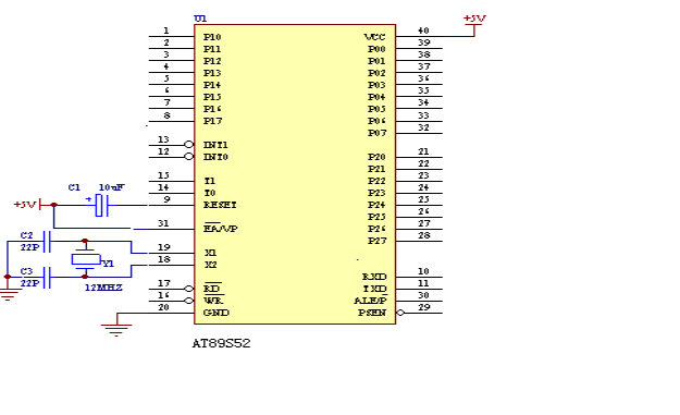 ⑴ 如图所示,图为单片机的基本外围电路。20管脚接地,40管脚接+5V电源,为单片机工作提供电源。18及19管脚接晶振,为单片机提供时钟信号,晶振为12MHz。晶振的振荡频率越高,系统的时钟频率越高,单片机工作的速度也越高。对于液晶显示电路的设计,需要单片机有较高的工作效率,所以选择比较高频率的晶振,从而提高液晶屏幕的刷新速率,获得更加连贯、流畅的图像显示。根据需要还可以加上复位电路,复位是单片机的初始化操作。或者当单片机程序运行出错导致死锁状态的时候,为摆脱困境,也需要按复位键以重新启动。
图2-2 AT89S52单片机基本外围电路

⑵ 如图2-3所示,左边为单片机模块,右边为液晶模块。单片机的P0口与液晶模块的8个数据端口相连,作为数据传送端口。 P2.4、5、7、8与液晶模块的片选CS1、CS2和R/W、D/I相连,作为控制字的写入。液晶模块的E端为使能端,由单片机的P2.3和P3.7、8三个口送信号至与非门驱动液晶模块,同时给使能端提供高低电平,控制液晶模块工作。液晶模块的VSS接地,VCC和V0接滑动变阻器,VCC接正5V电源,通过滑动变阻器分压,从而为液晶模块更好的工作提供电源,也作为液晶显示屏的亮度控制端。此图即为单片机控制液晶显示的基本电路。其中的与非门组合可以用74LS00芯片,74LS00可以提供3个与非门。本设计电路成本低,元件比较普通,市场上可以轻易买到,为整个设计提供方便。电路简单易于焊接,调试中也能减少很多麻烦。
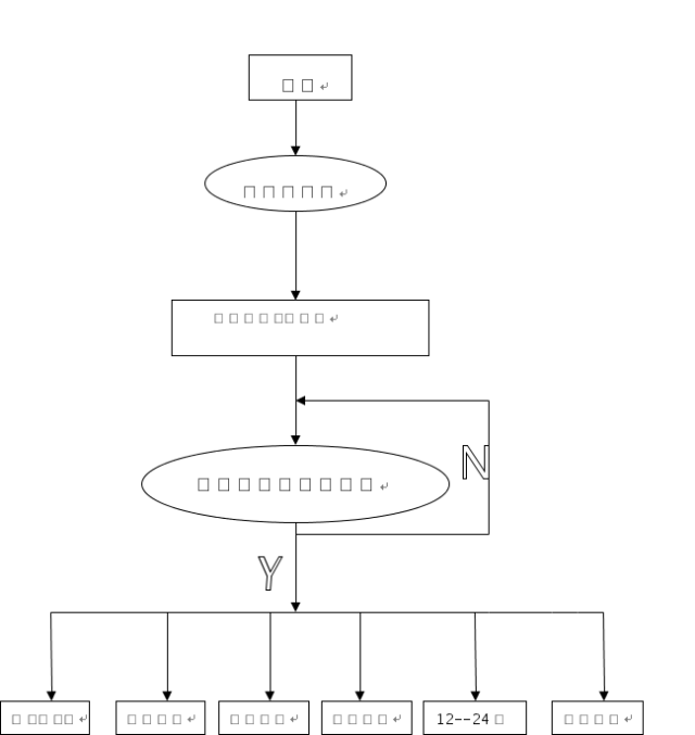
3. 方案设计与论证
按照系统设计功能的要求,初步确定设计系统由复位模块、时钟模块、音乐模块、光识模块及显示模块共五个模块组成,后来在时钟模块的基础上又加载了日历、星期的模块,为了使本设计中的数字钟的功能更加完善和强大,最后又将温度显示加入了设计方案中。
首先以单片机AT89S52为入手点,通过使用AT89S52的内部的可编程定时器/计数器,结合对外接晶振的调节来确定一个合适的振荡周期,从而确定出内部的机器周期。再通过对内部中断程序的设置来设计出时钟程序,即设计出了电子时钟的核心。
根据题目的要求,我设计了以下方案:
设计中加载了年、月、日的设计,刚开始时打算用18个共阳数码管,考虑到数码管太多是毕会给硬件电路带来麻烦,经过考虑后,决定把年、月、日与时间设置到一组数码管上来,即六个数码管即能显示时间又能显示年、月、日,这样一来就方便了硬件电路。
主控芯片使用51系列AT89S52单片机,温度模块设计中,温度元件采用AD590,利用AD590以及接口电路把温度转换成模拟电压,经由ADC0804转换成数字信号,然后经AT89S52处理显示温度。但由于AD590价钱比较贵,且只能转换成模拟电压,这样一来硬件就要增加更多的器件且又不经济,经查找发现18B20温度传感器价钱便宜且可以直接把温度转换成数字量测温范围为-55—125度,最大分辨率可达0.0625度,采用3线制与单片机相连,减少了外部的硬件电路,具有低成本和易使用的特点,所以我选择了18B20温度传感器。
在音乐模块的设计中,我决定采用音乐芯片,这样可以避免对铃声音乐的编程,即节省了时间,又减少了在程序中发生错误的可能性。
4. 系统总体结构框图
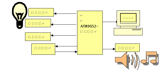
图4-1
在本设计中,以按键开关作为输入装置,LED七段数码显示管作为显示装置,因此,各按键开关的功能为:
S1键:P1.0口 时间调整
S2键:P1.1口 日期调整
S3健; p1.2口 闹铃设置
S4健: p1.3口 闹铃开关
5. 系统的硬件设计
电路是由控制部分和显示部分两大部分组成。利用单片机程序进行控制,并通过数码管进行显示。
5.1 显示部分电路的设计
5.1.1 LED数码显示管的基本原理
用单片机驱动LED数码管有很多方法,按显示方式分,有静态显示和动态显示,按译码方式可分为硬件译码和软件译码。
静态显示是显示驱动电路具有输出锁存功能,单片机将要显示的数据送出后不再控制LED,直到下次显示时再传送一次新的显示数据。静态显示的数据稳定,占用CPU时间少。
动态显示要CPU时刻对显示器件进行刷新,显示数据有闪烁感,占用CPU时间多。
这两种显示方式各有利弊:静态显示虽然数据显示稳定,占用很少的CPU时间,但每个显示单元都需要单独的显示驱动电路,使用的电路硬件较多;动态显示虽然有闪烁感,占用的CPU时间多,但使用的硬件少,能节省线路板空间。
动态扫描显示接口是单片机中应用最广泛的一种显示方式。其接口电路是把所有LED显示器的8个笔划段A~D、DP的同名端连在一起,而每一个数码管的公共端COM是各自独立地受I/O线控制。CPU向字段输出口送出字形码时,所有显示器接受到相同的字形码,但究竟是哪个显示器亮,则取决于COM端,而这一端是由I/O控制的,可以自行决定何时显示哪一位了。而所谓动态扫描就是指我们采用分时的方法,轮流控制各个显示器的COM端,是各个显示器轮流点亮。
在轮流点亮扫描过程中,每位显示器的点亮时间是极为短暂的,约1ms左右,但由于人的视觉暂留现象及发光二极管的余辉效应,尽管实际上各位显示器并非同时点亮,但只要扫描的速度足够快,给人的印象就是一组稳定的显示数据,不会有闪烁感。
从上述的论述中,可以看出动态显示方案具备一定的实用性,也是目前单片机数码管显示中较为常用的一种显示方法。所以,本设计也采用动态显示方案。
5.1.2 数码管显示模块分析
电路先通过电源电路送出+5V电压,单片机AT89S52通过74LS47和CD4515(4—16译码器)驱动数码管显示数值, 显示部分采用普通共阳极数码管显示,采用动态扫描,以减少硬件电路。考虑到一次扫描12位数码管显示时会出现闪烁情况,设计时分两排显示,一排显示时间和年月日,一排显示星期和温度, 共阳极数码管中8个发光
二极管的阳极(二极管正端)连在一起。通常,公共阳极接高电平(一般接电源),其它管脚接段驱动电路输出端。当某段驱动电路的输入端为低电平时,该端所连接的字段导通并点亮。根据发光字段的不同组合可显示出各种数字或字符。此时,要求段驱动电路能吸收额定的段导通电流,还需根据外接电源及额定段导通电流来确定相应的限流电阻。采用动态显示方式,比较节省I/O口,硬件电路也较静态显示简单,但其亮度不如静态显示方式,而且在显示位数较多时,CPU要依次扫描,占用CPU较多时间。
为了提供共阳LED数码管的驱动电压,用三极管9012作电源驱动输出。采用12MHz晶振,有利于提高秒计时的精确性。;
5.1.3 LED显示电路

图5-1
5.2 控制部分电路的设计
5.2.1 时钟模块
利用芯片内部的振荡器,然后在引脚XTAL1和引脚 XTAL2两端接晶体谐振器,就构成了稳定的自激振荡器,其发出的脉冲直接送入内部的时钟电路,如图外接晶振时,C1和C2的值通常选择30pF; C1、C2对频率有微调作用,晶体谐振器的频率12MHz。为了减少寄生电容,更好地保证振荡器稳定、可靠地工作,振荡器和电容应尽可能安装得与单片机芯片靠近。设置了12—24两种显示状态,调整计时的按键、设置定时的按键且定时设置了3次定时、还另加载了星期、年、月、日的调整及闰年的自动调整。
5.2.2 温度模块
主要由18B20通过单片机AT89S52中的温度程序不断的检测温度来显示温度。
18B20温度传感器工作原理:DS18B20温度传感器是美国DALLAS半导体公司最新推出的一种改进型智能温度传感器,与传统的热敏电阻等测温元件相比,它能直接读出被测温度,并可根据实际要求通过简单的编程实现9—12位的数字值读数方式,DS18B20的性能特点如下:
1、独特的单线接口仅需要一个引脚进行通信;
2、多个DS18B20可以并联在唯一的三线上,实现多点组网功能;
3、无须外部器件;
4、可通过数据线供电,电压范围为3.0---5.5V;
5、零待机功耗;
6、温度以9或12位数字量读出;
7、用户可定义的非易失性温度报警设置;
8、报警搜索命令识别并标志超过程序限定温度(温度报警条件)的器件;
9、负电压特性,电源极性接反是,温度计不会因发热而烧毁,但不能正常工作。
5.2.3 音乐模块
通过LM386N-1给扬声器信号来发出音乐,这个模块主要是为时钟定时到时发出音乐闹铃,而在软件部分设置了可以一次设置3次定时,每次定时到时,音乐程序中编了6种音乐,它可以自动选择6种音乐中的任一音乐响1分钟,如果中间不想让闹铃响可以按一按键,闹铃就立刻停止。
5.2.4 复位模块
单片机复位电路是使CPU和系统中的其他功能部件都处在一个确定的初始状态,并从该状态开始工作,例如复位后PC=0000H,使单片机从第一个单元取指令。无论是在单片机刚接上电源时,还是断电后或者发生故障后都要复位。
电路图为:

图5-2
5.2.5 光识模块
同样也是为定时服务的,只要定时到,组成心字的18只发光二极管就会按程序全亮全灭20次,如此循环。
电路图为:


图5-3
6. 系统的软件设计
6.1 各模块的程序设计
6.1.1 计时程序
计时程序是实现电子时钟的核心内容,本程序用中断time0来控制,计时显示的单元从50h开始,50h=秒的个位,51h=秒的十位,52h=分的个位,53h=分的十位,54h=时的个位,55h=时的十位
org 000bh
结 论
经过调试,和多次改进,本设计达到了预期的效果。数字钟可以正常显示时间和日期,并且对每个月份的天数进行了处理,特别是2月这个特殊月份,本设计可以自动从2月28日直接过度到3月1日。而且,在本设计中,闰年和平年的2月,其天数可以被正常区分,从而达到了实用和人性化的效果。对温度的显示也比较正常,能够正常反映出室温情况。当然,还可以根据需要,增加整点报时的功能,以使本设计更加完善。
总之,本设计提供了一套行之有效的数字钟的设计方案,并且成本较低,具有较高的实用性。
参考文献
[1] 卢坤,奚大顺电子设计技术[M].成都电子科技大学出版社,1997.P103-210
[2] 唐竞新.数字电子电路[M].第1版.北京:清华大学出版社,2003.P99-120
[3] 康华光.电子技术基础[M].数字部分.第4版.北京:高等教育出版社,1998.
P47-79
[4] 电子工程手册编委会等中外集成电路简明速查手册[M]---TTL,CMOS.北京:电子工业出版社,1991.P245-340
[5] 杨长春.论数字技术[J].《电子报》合订本.第0113期.成都:四川科学技术出版社,2002.12.P13-30
[6] 彭国贤.数码显示 [M].北京:电子工业出版社,1993.P21-50
[7] 康华光主编,邹寿彬副主编《电子技术基础(数字技术)》高等教育出版,2004.P129-180
[8] 康华光主编,陈大钦副主编《电子技术基础(模拟技术)》高等教育出版社,2003.P269-307
[9] 袁俊泉,孙敏琪,曹瑞编著 《数字系统设计及其应用》[J].《数字电子》第9908期. 西安电子科技大学出版社,2002.P13-26
[10] 李光飞、楼然苗等 《单片机课程设计实例指导》北京航空航天大学出版社,2004.P5-37
[11] 余永权.《ATMEL 系列Flash单片机原理及应用》北京:电子工业出版社,1997年第一版,P88~121
[12] 沙占友. 《智能化集成温度传感器原理与应用》北京:机械工业出版社,2002年第一版,P84~106
[13] 李广弟,朱月秀,王秀山.《单片机基础修订版》北京:北京航空航天大学出版社,2001年第二版,P11~77
[14] 蔡明生.《电子设计》北京:高等教育出版社,2004年第一版,P48~101
[15] 孙安青.《AT89S51单片机实验及实践教程》www.supermcu.com.P179~186
[16] 刘云,成后发,尹波.《温度无线传输技术的研究》电脑与信息技术,2004年第 4期,P47~50
[17] 陈跃东.《DS18B20集成温度传感器原理及其应用》 安徽机电学院学报,2002年第4期,P34~38
[18] 刘楚浩. 《用单片机实现温度远程显示》单片机与嵌入式系统应用.2002年第9期
[19] William Stallings.《Data and Computer Communications》.北京:高等教育出版社,2001年第一版
[20] CHEE-YEE CHONG,SRIKANTA PKUMAR. 《Sensor Networks:Evolution》,Opportunities and Challenges[A]. PROCEEDINGS OF THE IEEE[C]. 2003,91(8):1247-1256.
[21] Altera Corporation.2002. 《 Altera Digital Library.Altera》.P99-101
[22] Xilinx Inc.2001.Data Book 2001.Xilinx.P31-54
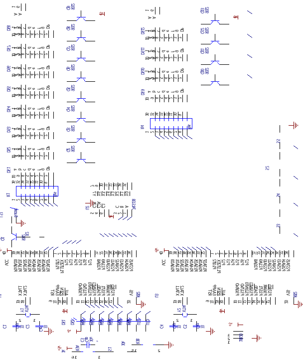
附录1 数字钟电路图
附录2 程序清单
org 0000h
jmp start
org 000bh
jmp time
org 30h
start: mov sp,#5fh ;// 小时 分钟 秒
mov r1,#0 ;// r2 r1 r5 r0 r3 r4
mov r2,#0
mov r7,#0
mov r0,#0
mov r6,#0
mov r5,#0
mov 20h,#31 ;//20h 日地址 日 月 年个位 年十位 年百位 年千位
mov 21h,#10 ;//21h 月地址 20h 21h 22h 23h 24h 25h
mov 22h,#6 ;//年个位
mov 23h,#0 ;//年十位
mov 24h,#0 ;//年百位
mov 25h,#2 ;/年千位
mov 34h,#0 ;//闹铃1 秒个位 时十位 时个位 分十位 分个位 秒十位 秒个位
mov 35h,#0 ;//闹铃1 秒十位
mov 36h,#1 ;//闹铃1 分个位 39h 38h 37h 36h 35h 34h
mov 37h,#0 ;//闹铃1 分十位
mov 38h,#0 ;//闹铃1 时个位
mov 39h,#0 ;//闹铃1 时十位 时十位 时个位 分十位 分个位 秒十位 秒个位
mov 49h,#1 ;//闹铃2 分个位 4ch 4bh 4ah 49h 48h 47h
mov 4ah,#0 ;//闹铃2 分十位
mov 4bh,#0 ;//闹铃2 时个位
mov 4ch,#0 ;//闹铃2 时十位
setb p1.5
mov TMOD,#00000001b
mov TH0,#3ch ;//定时器初值
mov TL0,#0b0h
setb EA ;//开总中断
setb ET0 ;//开定时器一的中断
mov p1,#0ffh
setb TR0 ;//定时器开始工作
k: mov 12h,r0
mov 13h,r1
mov 14h,r2 ; // 小时 分钟 秒
; // r2 r1 r5 r0 r3 r4
mov 15h,r5
; // 14h 13h 15h 12h
loop: mov r5,15h
mov r2,14h
mov r1,13h ;//地址中不是BCD码而是要显示的数字
mov r0,12h
mov a,r6 ; //R6中是秒脉冲个数
mov b,#10
div ab
mov dptr,#tab1 ; //商存在a中
movc a,@a+dptr
mov r3,a
mov a,b
movc a,@a+dptr ;//余数在b中
mov r4,a
mov dptr,#tab1
mov a,r0
movc a,@a+dptr ; //分 个位
mov r0,a
mov a,r5
movc a,@a+dptr ;//分 十位
mov r5,a; // 小时 分钟 秒
; // r2 r1 r5 r0 r3 r4
mov a,r1 ;
movc a,@a+dptr ;//时 个位 // 14h 13h 15h 12h
mov r1,a
; // 18h 17h 19h 16h
mov a,r2 ;//时 十位
movc a,@a+dptr; //此时地址中是要显示数字的BCD码
mov r2,a
mov 19h,r5
mov 18h,r2
mov 17h,r1
mov 16h,r0
mov 46h,r6
dsp:
mov p2,r4
mov p0,#70h ;//p0的高位接74LS138
lcall delay
mov p2,r3
mov p0,#60h
lcall delay
mov p2,r0 ;// 小时 分钟 秒
mov p0,#40h
lcall delay ; // r2 r1 r5 r0 r3 r4
;
mov p2,r5
mov p0,#30h
lcall delay
mov p2,r1
mov p0,#10h
lcall delay
mov p2,r2
mov p0,#00h
lcall delay
mov p0,#50h ;//在分与秒之间加 "一"
mov p2,#3fh
lcall delay
mov p0,#20h ;//在分与秒之间加 "一"
mov p2,#3fh
lcall delay
jnb p1.1,return1 ;//p1.1是年月日调整
jnb p1.0,jie ;//p1.0是时间调整
jnb p1.2,goto5 ;//p1.2进入闹铃
mov p3,#0ffh
call cheak2
call cheak3
call zcheak; //2ah.0为0跳转,不去整点报时
jb p1.5,out3
call cheak
out3: jb p1.6,out2
call cheak1
out2: jmp loop
goto6: mov p3,#150
ljmp notice
goto5: lcall delay1 ;// 跳往闹铃的按键防抖程序
jnb p1.2,goto6
ljmp loop
return5:mov P3,#190
ljmp showdate
return1:lcall delay1 ;/;/ 跳往日期调整的按键防抖程序
jnb p1.1,return5
ljmp loop
return8:mov p3,#230
ljmp dsp1
jie: lcall delay1 ;// 跳往时间调整的按键防抖程序
jnb p1.0,return8
ljmp loop
;//*************闹铃校对程序************************************************8
cheak: mov a,46h
cjne a,#0,out
mov a,36h ;//闹铃1比对,若成立就给P3口传入#00h
cjne a,12h,out
; 时十位 时个位 分十位 分个位 秒十位 秒个位
mov a,37h ;;39h 38h 37h 36h 35h 34h
cjne a,15h,out
mov a,38h
cjne a,13h,out
mov a,39h
cjne a,14h,out
mov a,36h ;4dh存闹铃1后一分的 分个位
inc a
mov 4dh,a
clr p1.7
clr p0.0
out: ret
cheak1: mov a,46h
cjne a,#0,out22
mov a,49h ;//闹铃1比对,若成立就给P3口传入#00h
cjne a,12h,out22
; 时十位 时个位 分十位 分个位 秒十位 秒个位
mov a,4ah ;;39h 38h 37h 36h 35h 34h
cjne a,15h,out22 ; 4ch 4bh 4ah 49h 48h 47h
mov a,4bh
cjne a,13h,out22
mov a,4ch
cjne a,14h,out22
mov a,49h
inc a
mov 4eh,a
clr p1.7
clr p0.0
out22: ret
;***************关闹铃报警******************************************************
;关闹铃一
cheak2: mov a,46h
cjne a,#0,out33
mov a,4dh ;//闹铃1比对,若成立就给P3口传入#00h
cjne a,12h,out33
; 时十位 时个位 分十位 分个位 秒十位 秒个位
mov a,37h ;;39h 38h 37h 36h 35h 34h
cjne a,15h,out33 ; 4ch 4bh 4ah 49h 48h 47h
mov a,38h
cjne a,13h,out33
mov a,39h
cjne a,14h,out33
setb p1.7
setb p0.0
out33: ret
;关闹铃二
cheak3: mov a,46h
cjne a,#0,out44
mov a,4eh ;//闹铃1比对,若成立就给P3口传入#00h
cjne a,12h,out44
; 时十位 时个位 分十位 分个位 秒十位 秒个位
mov a,4ah ;;39h 38h 37h 36h 35h 34h
cjne a,15h,out44 ; 4ch 4bh 4ah 49h 48h 47h
mov a,4bh
cjne a,13h,out44
mov a,4ch
cjne a,14h,out44
setb p1.7
setb p1.6
out44: ret
;********整点报时校对程序******************************************************************
; 小时 分钟
zcheak: mov a,46h
cjne a,#0,out
mov a,12h ; 14h 13h 15h 12h
cjne a,#0,out
mov a,15h
cjne a,#0,out
mov a,14h ;将原来存在13h,14h的小时转为一个值存在a中
mov b,#10
mul ab
add a,13h
cjne a,#1,play1
mov p3,#0
jmp out1
play1: cjne a,#2,play2
mov p3,#10
jmp out1
play2: cjne a,#3,play3
mov p3,#20
jmp out1
play3: cjne a,#4,play4
mov p3,#30
jmp out1
play4: cjne a,#5,play5
mov p3,#40
jmp out1
play5: cjne a,#6,play6
mov p3,#50
jmp out1
play6: cjne a,#7,play7
mov p3,#60
jmp out1
play7: cjne a,#8,play8
mov p3,#70
jmp out1
play8: cjne a,#9,play9
mov p3,#80
jmp out1
play9: cjne a,#10,play10
mov p3,#90
jmp out1
play10: cjne a,#11,play11
mov p3,#100
jmp out1
play11: cjne a,#12,play12
mov p3,#110
jmp out1
play12: cjne a,#13,play13
mov p3,#120
jmp out1
play13: cjne a,#14,play14
mov p3,#130
jmp out1
play14: cjne a,#15,play15
mov p3,#140
jmp out1
play15: cjne a,#16,play16
mov p3,#150
jmp out1
play16: cjne a,#17,play17
mov p3,#160
jmp out1
play17: cjne a,#18,play18
mov p3,#170
jmp out1
play18: cjne a,#19,play19
mov p3,#180
jmp out1
play19: cjne a,#20,play20
mov p3,#190
jmp out1
play20: cjne a,#21,play21
mov p3,#200
jmp out1
play21: cjne a,#22,play22
mov p3,#210
jmp out1
play22: cjne a,#23,play23
mov p3,#220
jmp out1
play23: cjne a,#24,out1
mov p3,#230
out1: ret
;闹铃调整
notice: mov dptr,#tab1
mov a,34h
movc a,@a+dptr ; 时十位 时个位 分十位 分个位 秒十位 秒个位
mov 45h,a
; 39h 38h 37h 36h 35h 34h
;BCD码 40h 41h 42h 43h 44h 45h
mov a,35h
movc a,@a+dptr ; 14h 13h 15h 12h
mov 44h,a
mov a,36h
movc a,@a+dptr
mov 43h,a
mov a,37h
movc a,@a+dptr
mov 42h,a
mov a,38h
movc a,@a+dptr
mov 41h,a
mov a,39h
movc a,@a+dptr
mov 40h,a
mov p2,45h
mov p0,#70h ;显示时间
lcall delay
mov p2,44h
mov p0,#60h
lcall delay
mov p2,43h
mov p0,#40h
lcall delay
mov p2,42h
mov p0,#30h
lcall delay ; 40h 41h 42h 43h 44h 45h
mov p2,41h
mov p0,#10h
lcall delay
mov p2,40h
mov p0,#00h
lcall delay
mov p0,#50h
mov p2,#3fh
lcall delay
mov p0,#20h
mov p2,#3fh
lcall delay
jnb p1.2,goto7 ; p1.2跳回
jnb p1.1,addfen ;p1.1分调整
jnb p1.0,addshi ;时调整
jnb p1.3,light ;开启或关闭闹铃
mov p3,#0ffh
jmp notice
goto8: mov p3,#170
jmp notice1
goto7: lcall delay1
jnb p1.2,goto8
ljmp notice
light: lcall delay1
lcall delay1
cpl p1.5
ljmp notice
addfen: call delay1
lcall delay1
mov r5,37h ; 39h 38h 37h 36h 35h 34h
mov r2,39h
mov r1,38h
mov r0,36h
inc r0 ; 小时 分钟 秒
cjne r0,#10,to ; r2 r1 r5 r0 r3 r4
mov r0,#0
inc r5 ; 14h 13h 15h 12h
cjne r5,#6,to
mov r5,#0
inc r1
cjne r1,#10,tiao
mov r1,#0
inc r2
tiao: cjne r2,#2,to
cjne r1,#4,to
mov r2,#0
mov r1,#0
to: mov 36h,r0
mov 38h,r1
mov 39h,r2
mov 37h,r5
ljmp notice
addshi: call delay1
lcall delay1
mov r5,37h ; 39h 38h 37h 36h 35h 34h
mov r2,39h
mov r1,38h
mov r0,36h
inc r1
cjne r1,#10,tiao1
mov r1,#0
inc r2
tiao1: cjne r2,#2,to1
cjne r1,#4,to1
mov r2,#0
mov r1,#0
to1: mov 36h,r0
mov 38h,r1
mov 39h,r2
mov 37h,r5
ljmp notice
;闹铃二设定
notice1:mov dptr,#tab1
mov a,34h
movc a,@a+dptr ; 时十位 时个位 分十位 分个位 秒十位 秒个位
mov 45h,a
; 39h 38h 37h 36h 35h 34h
; 4ch 4bh 4ah 49h 48h 47h
;BCD码 40h 41h 42h 43h 44h 45h
mov a,35h
movc a,@a+dptr ; 14h 13h 15h 12h
mov 44h,a
mov a,49h
movc a,@a+dptr
mov 43h,a
mov a,4ah
movc a,@a+dptr
mov 42h,a
mov a,4bh
movc a,@a+dptr
mov 41h,a
mov a,4ch
movc a,@a+dptr
mov 40h,a
mov p2,45h
mov p0,#70h ;显示时间
lcall delay
mov p2,44h
mov p0,#60h
lcall delay
mov p2,43h
mov p0,#40h
lcall delay
mov p2,42h
mov p0,#30h
lcall delay ; 40h 41h 42h 43h 44h 45h
mov p2,41h
mov p0,#10h
lcall delay
mov p2,40h
mov p0,#00h
lcall delay
mov p0,#50h
mov p2,#3fh
lcall delay
mov p0,#20h
mov p2,#3fh
lcall delay
jnb p1.2,goto9 ; p1.2跳回
jnb p1.1,addfen1 ;p1.1分调整
jnb p1.0,addshi1 ;时调整
jnb p1.3,light1
mov p3,#0ffh
jmp notice1
goto10: mov p3,#240
jmp loop
goto9: lcall delay1
jnb p1.2,goto10
ljmp notice1
light1: lcall delay1
lcall delay1
cpl p1.6
jmp notice1
addfen1:call delay1
lcall delay1
mov r5,4ah ; 39h 38h 37h 36h 35h 34h
mov r2,4ch ; 4ch 4bh 4ah 49h 48h 47h
mov r1,4bh
mov r0,49h
inc r0 ; 小时 分钟 秒
cjne r0,#10,to3 ; r2 r1 r5 r0 r3 r4
mov r0,#0
inc r5 ; 14h 13h 15h 12h
cjne r5,#6,to3
mov r5,#0
inc r1
cjne r1,#10,tiao3
mov r1,#0
inc r2
tiao3: cjne r2,#2,to3
cjne r1,#4,to3
mov r2,#0
mov r1,#0
to3: mov 49h,r0
mov 4bh,r1
mov 4ch,r2
mov 4ah,r5
ljmp notice1
addshi1:call delay1
lcall delay1
mov r5,4ah ; 39h 38h 37h 36h 35h 34h
mov r2,4ch ; 4ch 4bh 4ah 49h 48h 47h
mov r1,4bh
mov r0,49h
inc r1
cjne r1,#10,tiao4
mov r1,#0
inc r2
tiao4: cjne r2,#2,to4
cjne r1,#4,to4
mov r2,#0
mov r1,#0
to4: mov 49h,r0
mov 4bh,r1
mov 4ch,r2
mov 4ah,r5
ljmp notice1
dsp1:
mov r5,15h ; 小时 分钟 秒
mov r2,14h ; 14h 13h 15h 12h
mov r1,13h
mov r0,12h
;/* mov a,r6 ;
; mov b,#10
; div ab
; mov dptr,#tab1 ; r2 r1 r5 r0 r3 r4
; movc a,@a+dptr
; mov r3,a
;
; mov a,b
; movc a,@a+dptr
; mov r4,a
; */
mov dptr,#tab1
mov a,r0
movc a,@a+dptr ;计算BCD码
mov r0,a
mov a,r5
movc a,@a+dptr
mov r5,a
mov a,r1
movc a,@a+dptr
mov r1,a
mov a,r2
movc a,@a+dptr
mov r2,a
mov p2,r4
mov p0,#70h ;显示时间
lcall delay
mov p2,r3
mov p0,#60h
lcall delay
mov p2,r0
mov p0,#40h
lcall delay
mov p2,r5
mov p0,#30h
lcall delay
mov p2,r1
mov p0,#10h
lcall delay
mov p2,r2
mov p0,#00h
lcall delay
mov p0,#50h
mov p2,#3fh
lcall delay
mov p0,#20h
mov p2,#3fh
lcall delay
lcall delay
lcall delay
lcall delay
lcall delay
jnb p1.0,return2 ; p1.0跳回
jnb p1.1,fen ;p1.1分调整
jnb p1.2,shi
jnb p1.3,mon
mov p3,#0ffh
ljmp dsp1
return9:mov p3,#240;
jmp loop
return2:lcall delay1
jnb p1.0,return9
jmp dsp1
mon: mov p3,#222
call delay1
jmp dsp1
fen: call delay1
lcall delay1
mov r5,15h
mov r2,14h
mov r1,13h
mov r0,12h
inc r0 ; 小时 分钟 秒
cjne r0,#10,q ; r2 r1 r5 r0 r3 r4
mov r0,#0
inc r5
cjne r5,#6,q
mov r5,#0
inc r1
cjne r1,#10,next2
mov r1,#0
inc r2
next2: cjne r2,#2,q
cjne r1,#4,q
mov r2,#0
mov r1,#0
q: mov 12h,r0
mov 13h,r1
mov 14h,r2
mov 15h,r5
ljmp dsp1
shi: call delay1
lcall delay1
mov r5,15h
mov r2,14h ; 小时 分钟 秒
mov r1,13h ; r2 r1 r5 r0 r3 r4
mov r0,12h
inc r1
cjne r1,#10,next3
mov r1,#0
inc r2
next3: cjne r2,#2,pq
cjne r1,#4,pq
mov r2,#0
mov r1,#0
pq: mov 12h,r0
mov 13h,r1
mov 14h,r2
mov 15h,r5
ljmp dsp1
showdate:mov a,20h ; 日 月 年个位 年十位 年百位 年千位
mov b,#10 ; 20h 21h 22h 23h 24h 25h
div ab
mov dptr,#tab1
movc a,@a+dptr
mov 26h,a ;转化出来的BCD码
mov a,b ; 日个位 日十位
movc a,@a+dptr ; 27h 26h
mov 27h,a
mov a,21h
mov b,#10
div ab ; 月个位 月十位
movc a,@a+dptr
mov 28h,a ; 29h 28h
mov a,b
movc a,@a+dptr
mov 29h,a
mov a,22h
movc a,@a+dptr ; 年个位 年十位 年百位 年千位
mov 30h,a ; 22h 23h 24h 25h
;BCD码 30h 31h 32h 33h
mov a,23h
movc a,@a+dptr
mov 31h,a
mov a,24h
movc a,@a+dptr
mov 32h,a
mov a,25h
movc a,@a+dptr
mov 33h,a
jnb p1.1,goto2
jnb p1.2,goto4
mov p3,#0ffh
dsp5: mov p2,27h
mov p0,#70h ;年月日的BCD码
lcall delay ;日个位 日十位 月个位 月十位 年个位 年十位 年百位 年千位
;27h 26h 29h 28h 30h 31h 32h 33h
mov p2,26h
mov p0,#60h
lcall delay
mov p2,28h
mov p0,#40h
lcall delay
mov p2,30h
mov p0,#30h
lcall delay
mov p2,32h
mov p0,#10h
lcall delay
mov p2,33h
mov p0,#00h
lcall delay
mov p0,#50h
mov p2,29h
lcall delay
mov p0,#20h
mov p2,31h
lcall delay
jmp showdate
goto3: mov p3,#200
jmp date ;跳转到日期设置中
goto2: lcall delay1
jnb p1.1,goto3
ljmp showdate
goto4: lcall delay1
jmp loop
date: mov a,20h ; 日 月 年个位 年十位 年百位 年千位
mov b,#10 ; 20h 21h 22h 23h 24h 25h
div ab
mov dptr,#tab1
movc a,@a+dptr
mov 26h,a ;转化出来的BCD码
mov a,b ; 日个位 日十位
movc a,@a+dptr ; 27h 26h
mov 27h,a
mov a,21h
mov b,#10
div ab ; 月个位 月十位
movc a,@a+dptr
mov 28h,a ; 29h 28h
mov a,b
movc a,@a+dptr
mov 29h,a
mov a,22h
movc a,@a+dptr ; 年个位 年十位 年百位 年千位
mov 30h,a ; 22h 23h 24h 25h
;BCD码 30h 31h 32h 33h
mov a,23h
movc a,@a+dptr
mov 31h,a
mov a,24h
movc a,@a+dptr
mov 32h,a
mov a,25h
movc a,@a+dptr
mov 33h,a
jnb p1.1,return
jnb p1.0,adddate
jnb p1.2,decdate
mov p3,#0ffh
dsp2: mov p2,27h
mov p0,#70h ;年月日的BCD码
lcall delay ;日个位 日十位 月个位 月十位 年个位 年十位 年百位 年千位
;27h 26h 29h 28h 30h 31h 32h 33h
mov p2,26h
mov p0,#60h
lcall delay
mov p2,28h
mov p0,#40h
lcall delay
mov p2,30h
mov p0,#30h
lcall delay
mov p2,32h
mov p0,#10h
lcall delay
mov p2,33h
mov p0,#00h
lcall delay
mov p0,#50h
mov p2,29h
lcall delay
mov p0,#20h
mov p2,31h
lcall delay
jmp date
adddate:lcall delay1
lcall delay1 ;日加一
inc 20h
mov a,20h
cjne a,#32,over
mov 20h,#0
over: ljmp date
decdate:lcall delay1 ;日减一
lcall delay1
dec 20h
mov a,20h
cjne a,#-1,over
mov 20h,#31
jmp over
return6:mov p3,#210
jmp r ;跳转到日
return: lcall delay1
mov p3,#230
jnb p1.1,return6
ljmp date
r: mov a,20h
mov b,#10 ;日 月 年个位 年十位 年百位 年千位
div ab ;20h 21h 22h 23h 24h 25h
mov dptr,#tab1
movc a,@a+dptr
mov 26h,a
mov a,b
movc a,@a+dptr
mov 27h,a
mov a,21h
mov b,#10
div ab
movc a,@a+dptr
mov 28h,a
mov a,b
movc a,@a+dptr
mov 29h,a
mov a,22h
movc a,@a+dptr
mov 30h,a
mov a,23h
movc a,@a+dptr
mov 31h,a
mov a,24h
movc a,@a+dptr
mov 32h,a
mov a,25h
movc a,@a+dptr
mov 33h,a
jnb p1.1,back1
jnb p1.0,addri
jnb p1.2,decri
mov p3,#0ffh
dsp3: mov p2,27h
mov p0,#70h
lcall delay
mov p2,26h
mov p0,#60h
lcall delay
mov p2,28h
mov p0,#40h
lcall delay
mov p2,30h
mov p0,#30h
lcall delay
mov p2,32h
mov p0,#10h
lcall delay
mov p2,33h
mov p0,#00h
lcall delay
mov p0,#50h
mov p2,29h
lcall delay
mov p0,#20h
mov p2,31h
lcall delay
jmp r
addri: lcall delay1
lcall delay1
inc 21h
mov a,21h
cjne a,#13,over1
mov 21h,#1
over1: ljmp r
decri: lcall delay1
lcall delay1
dec 21h
mov a,21h
cjne a,#0,over1
mov 21h,#12
jmp over1
back: mov P3,#220 ;跳转年调整,此俩个back 为按键防抖
jmp nian
back1: lcall delay1
jnb p1.1,back
ljmp dsp3
nian: mov a,20h ; 日 月 年个位 年十位 年百位 年千位
mov b,#10 ; 20h 21h 22h 23h 24h 25h
div ab
mov dptr,#tab1
movc a,@a+dptr
mov 26h,a ;转化出来的BCD码
mov a,b ; 日个位 日十位
movc a,@a+dptr ; 27h 26h
mov 27h,a
mov a,21h
mov b,#10
div ab ; 月个位 月十位
movc a,@a+dptr
mov 28h,a ; 29h 28h
mov a,b
movc a,@a+dptr
mov 29h,a
mov a,22h
movc a,@a+dptr ; 年个位 年十位 年百位 年千位
mov 30h,a ; 22h 23h 24h 25h
;BCD码 30h 31h 32h 33h
mov a,23h
movc a,@a+dptr
mov 31h,a
mov a,24h
movc a,@a+dptr
mov 32h,a
mov a,25h
movc a,@a+dptr
mov 33h,a
dsp4: mov p2,27h
mov p0,#70h ;年月日的BCD码
lcall delay ;日个位 日十位 月个位 月十位 年个位 年十位 年百位 年千位
;27h 26h 29h 28h 30h 31h 32h 33h
mov p2,26h
mov p0,#60h
lcall delay
mov p2,28h
mov p0,#40h
lcall delay
mov p2,30h
mov p0,#30h
lcall delay
mov p2,32h
mov p0,#10h
lcall delay
mov p2,33h
mov p0,#00h
lcall delay
mov p0,#50h
mov p2,29h
lcall delay
mov p0,#20h
mov p2,31h
lcall delay
jnb p1.1,goto
jnb p1.0,addnian
jnb p1.2,decnian
mov p3,0ffh
jmp nian
addnian:lcall delay1
lcall delay1 ;年个位 年十位 年百位 年千位
inc 22h ;22h 23h 24h 25h
mov a,22h
cjne a,#10,over4
mov 22h,#0
inc 23h
mov a,23h
cjne a,#10,over4
mov 23h,#0
inc 24h
mov a,24h
cjne a,#10,over4
mov 24h,#0
inc 25h
mov a,25h
cjne a,#10,over4
mov 25h,#0
over4: jmp nian
decnian:lcall delay1
lcall delay1 ;年个位 年十位 年百位 年千位
dec 22h ;22h 23h 24h 25h
mov a,22h
cjne a,#-1,over4
mov 22h,#0
dec 23h
mov a,23h
cjne a,#-1,over4
mov 23h,#0
dec 24h
mov a,24h
cjne a,#-1,over4
mov 24h,#0
dec 25h
mov a,25h
cjne a,#-1,over4
mov 25h,#0
jmp over4
goto1: mov p3,#240
jmp loop ;跳转到日
goto: lcall delay1
jnb p1.1,goto1
ljmp nian
time: mov r5,15h
mov r2,14h ;秒脉冲得到后,软件计算时间
mov r1,13h
mov r0,12h
inc r7
mov a,r7
cjne a,#20,T_ret
inc r6
cjne r6,#60,t
mov r6,#0
inc r0
cjne r0,#10,t
mov r0,#0
inc r5
cjne r5,#6,t
mov r5,#0
inc r1
cjne r1,#10,next1
mov r1,#0
inc r2
next1: cjne r2,#2,t
cjne r1,#4,t
mov r2,#0
mov r1,#0
inc 20h
mov p3,#222
call delay1
mov a ,20h
cjne a,#32,t
mov 20h,#1
inc 21h
mov a,21h
cjne a,#13,t
mov 21h,#1
inc 22h
;/* cjne r1,#24,ask
; mov r1,#0
;ask: mov dptr,#tab1
; mov a,r1
; mov b,#10
; div ab
; movc a,@a+dptr
; add a,r2
; mov r2,a
; mov a,b
; movc a,@a+dptr
; add a,r1
; mov r1,a */
t: mov r7,#0
T_ret: mov TH0,#03ch
mov TL0,#0b0h
mov 12h,r0
mov 13h,r1
;将算出来的时间赋回地址中
mov 14h,r2 ; 小时 分钟 秒
; r2 r1 r5 r0 r3 r4
mov 15h,r5
reti
delay: mov 10h,#4
d3: mov 11h,#5
d4: djnz 11h,d4
djnz 10h,d3
ret
delay1: mov 10h,#0bfh
d1: mov 11h,#0ffh
d2: djnz 11h,d2
djnz 10h,d1
ret
tab1: db 0c0h,0f9h,0a4h,0b0h,99h,92h,82h,0f8h,00h,90h
end
(3)控制附机的的程序
#include"reg52.h"
sbit warmer=P2^4;
sbit led_run=P2^0;
sbit k_power=P2^5;
sbit P3_0=P3^0 ;
sbit P3_2=P3^2 ;
sbit P3_3=P3^3 ;
sbit P3_4=P3^4 ;
sbit P3_5=P3^5 ;
sbit day=P2^7 ;
sbit ge=P3^7;
sbit shi=P3^6;
sbit DQ =P3^1; //定义通信端口
int play() //语音芯片控制位
{
P3_0=1;
P3_2=0;
P3_3=0;
P3_4=0;
P3_5=0;
P3_3=1;
}
//延时函数
unsigned char tab[]={0xc0,0xf9,0xa4,0xb0,0x99,0x92,0x82,0xf8,0x80,0x90,0xbf};
//0, 1, 2 3 4 5 6 7 8 9
void delay(unsigned int i)
{
while(i--);
}
//初始化函数
Init_DS18B20(void)
{
unsigned char x=0;
DQ = 1; //DQ复位
delay(8); //稍做延时
DQ = 0; //单片机将DQ拉低
delay(80); //精确延时 大于 480us
DQ = 1; //拉高总线
delay(14);
x=DQ; //稍做延时后 如果x=0则初始化成功 x=1则初始化失败
delay(20);
}
//读一个字节
ReadOneChar(void)
{
unsigned char i=0;
unsigned char dat = 0;
for (i=8;i>0;i--)
{
DQ = 0; // 给脉冲信号
dat>>=1;
DQ = 1; // 给脉冲信号
if(DQ)
dat|=0x80;
delay(4);
}
return(dat);
}
//写一个字节
WriteOneChar(unsigned char dat)
{
unsigned char i=0;
for (i=8; i>0; i--)
{
DQ = 0;
DQ = dat&0x01;
delay(5);
DQ = 1;
dat>>=1;
}
delay(4);
}
//读取温度
ReadTemperature(void)
{
unsigned char a=0;
unsigned char b=0;
unsigned char t=0;
Init_DS18B20();
WriteOneChar(0xCC); // 跳过读序号列号的操作
WriteOneChar(0x44); // 启动温度转换
Init_DS18B20();
WriteOneChar(0xCC); //跳过读序号列号的操作
WriteOneChar(0xBE); //读取温度寄存器等(共可读9个寄存器) 前两个就是温度
a=ReadOneChar(); //读取温度值低位
b=ReadOneChar(); //读取温度值高位
a=a>>4; //低位右移4位,舍弃小数部分
t=b<<4; //高位左移4位,舍弃符号位
t=t|a;
return(t);
}
void display_tempmain(unsigned char i) //主程序温度显示函数
{
P2=tab[i/10];
shi=0;
ge=1;
day=1;
delay(500);
P2=tab[i%10];
shi=1;
ge=0;
day=1;
delay(500);
}
void main(void)
{unsigned int temp;
int play();
unsigned int i,j=2;
while(1) //主循环
{ temp=ReadTemperature();
display_tempmain(temp);
P2=tab[j];
shi=1;
ge=1;
day=0;
if(P0==222){
j++;
if(j==8){
j=1;
}
for(i=40000;i>0;i--);
}
if(P0==0x00){
P1=250;
play();
for(i=60000;i>0;i--);
for(i=60000;i>0;i--);
//语音地址 0 10 20 30 40 50 60 70 80 90 (十进制)
P1=0x00;
play();
//语音地址 100 110 120 130 140 150 160 170 180 190 200 210 220 230
}
if(P0==10){ //跳出 现在时刻
P1=250;
play();
for(i=60000;i>0;i--);
for(i=60000;i>0;i--);
// 240 250
P1=10;
play();
}
if(P0==20){
P1=250;
play();
for(i=60000;i>0;i--);
for(i=60000;i>0;i--);
P1=20;
play();
}
if(P0==30){
P1=250;
play();
for(i=60000;i>0;i--);
for(i=60000;i>0;i--);
P1=30 ;
play();
}
if(P0==40){
P1=250;
play();
for(i=60000;i>0;i--);
for(i=60000;i>0;i--);
P1=40;
play();
}
if(P0==50){
P1=250;
play();
for(i=60000;i>0;i--);
for(i=60000;i>0;i--);
P1=50;
play();
}
if(P0==60){
P1=250;
play();
for(i=60000;i>0;i--);
for(i=60000;i>0;i--);
P1=60 ;
play();
}
if(P0==70){
P1=250;
play();
for(i=60000;i>0;i--);
for(i=60000;i>0;i--);
P1=70 ;
play();
}
if(P0==80){
P1=250;
play();
for(i=60000;i>0;i--);
for(i=60000;i>0;i--);
P1=80;
play();
}
if(P0==90){
P1=250;
play();
for(i=60000;i>0;i--);
for(i=60000;i>0;i--);
P1=250;
play();
for(i=60000;i>0;i--);
for(i=60000;i>0;i--);
P1=90 ;
play();
}
if(P0==100){
P1=250;
play();
for(i=60000;i>0;i--);
for(i=60000;i>0;i--);
P1=100;
play();
}
if(P0==110){
P1=250;
play();
for(i=60000;i>0;i--);
for(i=60000;i>0;i--);
P1=110;
play();
}
if(P0==120){
P1=250;
play();
for(i=60000;i>0;i--);
for(i=60000;i>0;i--);
P1=120;
play();
}
if(P0==130){
P1=250;
play();
for(i=60000;i>0;i--);
for(i=60000;i>0;i--);
P1=130;
play();
}
if(P0==140){
P1=250;
play();
for(i=60000;i>0;i--);
for(i=60000;i>0;i--);
P1=140 ;
play();
}
if(P0==150){
P1=150;
play();
}
if(P0==170){
P1=170 ;
play();
}
if(P0==190){
P1=190 ;
play();
}
if(P0==200){
P1=200;
play();
}
if(P0==210){
P1=210;
play();
}
if(P0==220){
P1=220;
play();
}
if(P0==230){
P1=230;
play();
}
if(P0==240){
P1=240;
play();
}
附录3 英文资料
Power Management Techniques and Calculation
Relevant Devices
This application note applies to the following devices: C8051F000, C8051F001, C8051F002, C8051F005, C8051F006, C8051F010, C8051F011, C8051F012, C8051F012, C8051F015, C8051F016, and C8051F017.
Introduction
This application note discusses power management techniques and methods of calculating power in a Cygnet C8051F00x and C8051F01x Sock. Many applications will have strict power requirements, and there are several methods of lowering the rate of power consumption without sacrificing performance. Calculating the predicted power use is important to characterize the system’s power supply requirements.
Key Points
• Supply voltage and system clock frequency strongly affect power consumption.
• Cygnet’s Sock’s feature power management modes: IDLE and STOP.
• Power use can be calculated as a function of system clock frequency, supply voltage, and enabled peripherals.
Power Saving Methods
CMOS digital logic device power consumption is affected by supply voltage and system clock (SYSCLK) frequency. These parameters can be adjusted to realize power savings, and are readily controlled by the designer. This section discusses these parameters and how they affect power usage.
Reducing System Clock Frequency
In CMOS digital logic devices, power consumption is directly proportional to system clock (SYSCLK) frequency: power=CV2ƒ, where C is CMOS load capacitance, V is supply voltage, and ƒ is SYSCLK frequency.
Equation 1.CMOS Power Equation
The system clock on the C8051Fxxx family of devices can be derived from an internal oscillator or an external source. External sources may be a CMOS clock, RC circuit, capacitor, or crystal oscillator. For information on configuring oscillators, see application note: “AN02 - Configuring the Internal and External Oscillators.” The internal oscillator can provide four SYSCLK frequencies: 2, 4, 8, and16 MHz. Many different frequencies can be achieved using the external oscillator.
To conserve power, a designer must decide what the fastest needed SYSCLK frequency and required accuracy is for a given application. A design may require a constant SYSCLK frequency during all device operations. In this case, the designer will choose the lowest possible frequency required, and use the oscillator configuration that consumes the least power. Typical applications include serial communications, and periodic sampling with an ADC that must be performed.
Some operations may require high speed operation, but only in short, intermittent intervals. This is sometimes referred to as “burst” operation. In the C8051Fxxx, the SYSCLK frequency can be changed at anytime. Thus, the device can operate at low frequency until a condition occurs that requires high frequency operation.
Two examples of alternating between SYSCLK sources are (1) an internal oscillator/external crystal configuration, and (2) an external crystal/RC oscillator configuration. If the device is used for occasional high speed data conversion, and a real-time clock is used for time-stamping the data, a combination internal oscillator and external crystal would be ideal. During sampling operations, the high speed internal oscillator would be used. When sampling is complete, the device could then use an external 32 kHz crystal to maintain the real-time clock. Once high speed operations are required again, the device switches to the internal oscillator as necessary (see Figure 1below). An example of this procedure is illustrated in application note “AN008 Implementing a Real-Time Clock”.
The crystal oscillator and internal oscillator may be operated simultaneously and each selected as the SYSCLK source in software as desired. To reduce supply current, the crystal may also be shutdown when using the internal oscillator. In this case, when switching from the internal to external oscillator the designer must consider the start-up delay when switching the SYSCLK source. The C8051F0xx devices have a flag that is set when the external clock signal is valid (XTLVLD bit in the OSCXCN register) to indicate the oscillator is running and stable. This flag is polled before switching to the external oscillator. Note that other operations can continue using the internal oscillator during the crystal start-up time.
Some applications require intermittent high speed and accuracy (e.g., ADC sampling and data processing), but have lower frequency and accuracy requirements at other times (e.g., waiting for sampling interval), a combination of an external oscillator and RC circuit can be useful. In this case, the external RC oscillator is used to derive the lower frequency SYSCLK source, and the crystal is used for high frequency operations. The RC circuit requires a connection to VDD (voltage source) to operate.

Because this connection could load the crystal oscillator circuit while the crystal is in operation, we connect the RC circuit to a general purpose port pin (see Figure 2 below). When the RC circuit is in use, the port pin connection is driven high (to VDD) by selecting its output mode to “push-pull” and writing a ‘1’ to the port latch. When the crystal oscillator is being used, the port pin is placed in a ‘hi- Z’ condition by configuring the output mode of the port to “open-drain” and writing a ‘1’ to the port latch. Note the RC circuit may take advantage of the existing capacitors used for the crystal oscillator.
The start-up of the RC-circuit oscillator is nearly instantaneous. However, there is a notable start-up time for the crystal. Therefore, switching from the RC oscillator to the external crystal oscillator using the following procedure:
1. Switch to the internal oscillator.
2. Configure the port pin used for the RC circuit voltage supply as open-drain and write a ‘1’ to the port pin (Hi-Z condition).
3. Start the crystal (Set the XFCN bits).
4. Wait for 1 ms.
5. Poll for the External Crystal Valid Bit (XTLVLD --> ‘1’).
6. Switch to the external oscillator.
Switch from the external crystal oscillator to the RC oscillator as follows:
1. Switch to the internal oscillator.
2. Shutdown the crystal (clear the XFCN bits).
3. Drive the voltage supply port pin high (to VDD) by putting the port pin in “push pull” mode and writing a ‘1’ to its port latch.
4. Switch back to the external oscillator.

Supply Voltage
The amount of current used in CMOS logic is directly proportional to the voltage of the power supply. The power consumed by CMOS logic is proportional the power supply voltage squared (See Equation 1). Thus, power consumption may be reduced by lowering the supply voltage to the device. The C8051Fxxx families of devices require a supply voltage of 2.7-3.6 Volts. Thus, to save power, it is recommended to use a 3.0 volt regulator instead of a 3.3 volt regulator for power savings.
CIP-51 Processor Power Management Modes
The C8051 processor has two modes which can be used for power management. These modes are IDLE and STOP.
IDLE Mode
In IDLE Mode, the CPU and FLASH memory are taken off-line. All peripherals external to the CPU remain active, including the internal clocks. The CPU exits IDLE Mode when an enabled interrupt or reset occurs. The CPU is placed in IDLE Mode by setting the Idle Mode Select Bit (PCON.0) to ‘1’.
When the IDLE Mode Select Bit is set to ‘1’, the CPU enters IDLE Mode once the instruction that sets the bit has executed. An asserted interrupt will clear the IDLE Mode Select Bit and the CPU will vector to service the interrupt. After a return from interrupt (RETI), the CPU will return to the next instruction following the one that had set the IDLE Mode Select Bit. If a reset occurs while in IDLE Mode, the normal reset sequence will occur and the CPU will begin executing code at memory location 0x0000.
As an example, the CPU can be placed in IDLE while waiting for a Timer 2 overflow to
Initiate a sample/conversion in the ADC. Once the conversion and sample processing is complete, the ADC end-of-conversion interrupt wakes the CPU from IDLE Mode and processes the sample. After the sample processing is complete, the CPU is placed back into IDLE Mode to save power while waiting for the next interrupt.
As another example, the CPU may wait in IDLE Mode to save power until an external
Interrupt signal is used to “wake up” the CPU as needed. Upon receiving an external interrupt, the CPU will exit IDLE Mode and vector to the corresponding interrupt vector (e.g., / INT0 or /INT1).
STOP Mode
The C8051 STOP Mode is used to shut down the CPU and oscillators. This will effectively shut down all digital peripherals as well. All analog peripherals must be shutdown by software prior to entering STOP Mode. The processor exits STOP Mode only by an internal or external reset. Thus, STOP Mode saves power by reducing the SYSCLK frequency to zero.
Note that the Missing Clock Detector will cause an internal reset (if enabled) that will terminate STOP Mode. Thus, the Missing Clock Detector should be disabled prior to entering STOP Mode if the CPU is to be in STOP Mode longer than the Missing Clock Detector timeout (100 μs).
The C8051 processor is placed in STOP Mode by setting the STOP Mode Select Bit (PCON.1) to ‘1’. Upon reset, the CPU performs the normal reset sequence and begins executing code at 0x0000. Any valid RESET source will exit STOP Mode. Sources of reset to exit STOP Mode are External Reset (/RST), Missing Clock Detector, Comparator 0, and the External ADC Convert Start (/CNVSTR).
As an example, the CPU may be placed in STOP Mode for a period to save power when no device operation is required. When the device is needed, Comparator 0 reset could be used to “wake up” the device.
Generally, a power conscious design will use the lowest voltage supply, lowest SYSCLK frequency, and will use Power Management Modes when possible to maximize power savings. Most of these can be implemented or controlled in software.
Calculating Power Consumption
There are two components of power consumption in Cygnet’s C8051F00x and C8051F01x family of devices: analog and digital. The analog component of power consumption is nearly constant for all SYSCLK frequencies. The digital component of power consumption changes considerably with SYSCLK frequency. The digital and analog components are added to determine the total power consumption.
The current use calculations presented in this application note apply to the C8051F00x and C8051F01x (‘F000, 01, 02, 03, 05, 06, 10, 11, 12, 15, and 16) family of Cygnet devices.
The data sheet section, “Global DC Electrical Characteristics” contains various supply current values for different device conditions. The current values are separated into digital (at three example frequencies) and analog components. The analog numbers presented are values with all analog peripherals active. Supply current values for each analog peripheral can be found in the data sheet section for the peripheral.
For convenience, the Global DC Electrical Characteristics for the C8051F00x and C8051F01x family of devices are presented in the table below.
Internal vs. External Oscillator
Besides using lower SYSCLK frequencies, the designer can realize power savings by making smart SYSCLK source choices. The internal oscillator will typically consume 200μA of current supplied from the digital power supply. The current used to drive an external oscillator can vary. The drive current (supplied from the analog power supply) for an external source, such as a crystal, is set in software by configuring the XFCN bits in the External Oscillator Control Register (OSCXCN). Thus, at higher drive currents the user may save power by using the internal oscillator. However, at the lowest XFCN setting the external oscillator will use less than 1μA which is less current than used by the internal oscillator. Some typical measured current values are listed below. These measurements may vary from device to device. This drive level is kept as low as possible
To minimize power consumption, but must be high enough to start the external oscillator. The following table lists the current vs. External Oscillator Frequency Control Bit settings.
Digital Peripherals
For rough calculations, a good rule of thumb is to assume a 1mA/MHz of operating current (digital) + 1mA if the analog components (ADC, comparators, DAC, VREF, etc.) are enabled. This rule of thumb assumes a 3.6 V supply voltage. A lower supply voltage will reduce power consumption. At 2.7 V, the rule of thumb is 0.5mA/MHz (in NORMAL mode). The rules of thumb for rough calculations are presented in the table below:
Analog Peripherals
The individual supply current values for each analog peripheral are posted in the data sheet section for that component (typically near the end of the section). It is recommended to disable all peripherals not in use to save power. For convenience, the C8051F00x and C8051F10x analog peripherals supply current values are listed below:
Calculating Total Current
When the required SYSCLK frequency, supply voltage, and peripherals have been determined, the total supply current can be estimated. To calculate the total supply current, the analog peripheral current use (found by adding the currents of each of the enabled analog peripherals) is added to the digital current use (calculated for a given frequency, power mode, and supply voltage). If all of the analog peripherals are enabled, analog current use is about 1mA.
Example Calculations
The following are examples of supply current calculations. Each application may use different power modes, SYSCLK frequencies, and peripherals at different times. Thus, power management specifications may require several different supply current calculations. The digital component and analog components of current use are found separately, and then added together for the total.
Example 1
The C8051F000 device is being used in a system with VDD=3.6 V. An ADC is sampling parameters and processing the sample for an output to one DAC. Because of the sampling and processing requirements of the application, SYSCLK frequency is 16 MHz using the internal oscillator.
Analog Components
Peripheral Supply Current (μ A)
ADC 450
VREF (internal) 50
Internal Oscan. 200
One DAC 110
VDD monitor 15
Total Analog 825
Digital Component
In NORMAL Mode @ 16 MHz;
1mA/M Hz * 16 MHz = 16mA
Total
825μA (analog) + 16mA (digital)= 16.8mA
Example 2
Assume we are still estimating the supply current in the same application in Example 1. If the sample processing is a burst operation (i.e., intermittent need for sampling and conversions), we may choose to place the CIP-51 in IDLE Mode to allow a Timer to wake-up the CIP-51 after a specified interval. In this case, the average supply current can be calculated in order to estimate power requirements. The device will switch between NORMAL Mode (for sampling and data conversion) and IDLE Mode (between sample processing operations). The switch between IDLE and NORMAL Modes (and supply current values) will happen in a cycle with a period equal to the sampling rate. (See Figure 3 below). This will allow us to calculate average supply current, after we calculate the supply current in IDLE Mode.
Analog Component
Analog peripherals are disabled during the IDLE Mode period between sample processing and output. Thus, analog current consumption is just:
VDD monitor = 15μA.
Digital Component
In IDLE Mode @ 16 MHz;
0.65mA/MHz * 16 MHz = 10.4mA
Total
The analog component would be considered negligible in most applications, thus, the total is just the digital component:
50μA (analog) + 10.4mA (digital) = 10.4mA
Now that we have calculated IDLE Mode supply current and NORMAL Mode supply current (in Example 1), we must calculate the time we spend in each mode to find the average current the device will use.
Assuming the ADC is in low-power tracking mode and at the maximum SAR conversion
Clock of 2 MHz (ADC set for SAR clock = SYSCLK/8), and we desire a 10 kHz sampling rate. The period of the power cycle in Figure 3 is 1/10,000 (sample rate) = 100μs.
The time in NORMAL Mode will be the ADC tracking/conversion time, and the time to store the value in memory. In low-power tracking mode, it will take 3 SAR clocks for tracking, and 16 SAR clocks for conversion. 19 SAR clocks at 2 MHz will take 9.5μs. To store the number will take to system clock cycles, or 0.125μs. To enter NORMAL Mode, a move instruction is executed, taking 3 SYSCLK cycles which takes 0.188μs. Thus, the total time in NORMAL Mode is 9.5 μs+0.125 μs+0.188μs = 9.8μs.
Because the ADC sample period is 100μs, the time we may be in IDLE Mode during the power cycle is 100μs - 9.8μs (time in NORMAL Mode) = 90.2μs. By integrating the area under the curve in Figure 3 for one period (100μs), and dividing that number by the period, the average supply current is 11mA.

Example 3
If the oscillator frequency were lowered while in IDLE Mode (in Example 2) to 32 kHz using an external crystal for additional power savings, the current use would be:
The external oscillator control bits will be set to XFCN = 000. This uses 0.6μA of analog current. (0.65mA *.032 MHz) + 0.6μA = 21μA
This is a dramatic difference from Example 2’s IDLE Mode at 16 MHz, by simply reducing oscillator frequency.
Continuing with the average supply current calculation in Example 2 (with 6 extra SYSCLK cycles in NORMAL Mode to lower the frequency), the average supply current would be 1.7mA!
Example 4
In this application, the C8051F000 is being used to sample a parameter using the ADC and store samples in memory, with high accuracy timing of samples required. For more accurate timing, the SYSCLK is derived from an external 18.432 MHz crystal oscillator. To save power, the designer has decided to use a supply voltage of 3.0 V. Timer 2 is used to time the ADC sampling intervals.
Digital Component
In NORMAL Mode @ 18.432 MHz;
0.8mA/MHz * 18.432 MHz = 14.7mA
Total Current Use
3.4mA (analog)+14.7mA (digital)= 18.1mA
Example 4 in IDLE Mode
Placing the application in IDLE Mode with the ADC disabled during intervals that sampling is not required (no CIP-51 operations are needed; digital peripherals continue to operate) will save power if the sampling operation is a burst operation. In IDLE Mode, the digital current consumption is only 0.6mA/MHz, with no ADC, thus the current consumption at 18.432 MHz =11.1 miscalculating the average supply current for one sample period (similarly to Example 2, assuming a 10 kHz sampling rate and low-power tracking mode), the average current is estimated to be 11.9mA
附录4 英文资料翻译
电源管理技术及计算
本设计应用于下列器件
C8051F000、C8051F001、C8051F002、C8051F005、C8051F006、C8051F010、C8051F011、C8051F012、C8051F015、C8051F016、C8051F017
1 引言
本应用笔记讨论电源管理技术及计算C8051F00x和C8051F01x Sock中的功率消耗的方法。很多应用系统对功耗有严格的要求,也存在几种不以牺牲性能为代价的降低功耗的方法,计算预计功耗对于说明系统的供电要求是很重要的 。
2 关键点
供电电压和系统时钟频率对功率消耗有很大影响 。
Cygnet的Sock有两种电源管理方式等待和停止。
功率消耗可以作为系统时钟电源电压和被允许的外设的函数来计算。
3 降低功耗的方法
CMOS数字逻辑器件的功耗受供电电压和系统时钟(SYSCLK)频率的影响。可以通过调整这些参数来降低功耗,设计者也很容易控制这些参数。本节讨论这些参数及它们对功率消耗的影响 。
4 降低系统时钟频率
在CMOS数字逻辑器件中,功耗与系统时钟(SYSCLK)频率成正比:
功耗 = CV2f
其中C是CMOS的负载电容,V是电源电压,f是SYSCLK的频率 。
C8051Fxxx系列器件的系统时钟可以来自内部振荡器或一个外部时钟源。外部源可以是一个CMOS时钟、RC电路、电容或晶体振荡器。有关振荡器配置方面的信息见应用笔记–“ 配置内部和外部振荡器”。内部振荡器可提供四个时钟频率2、4、8 和16 MHz。很多不同的频率可以通过使用外部振荡器得到,为了节省功耗设计者必须知道给定应用所需要的最高SYSCLK频率和精度。一个设计可能需要一个在器件全部工作时间内保持不变的SYSCLK频率。在这种情况下,设计者将选择满足要求的最低频率,采用消耗最低功率的振荡器配置。典型的应用包括串行通信和必须用ADC完成的周期性采样。
某些操作可能要求高速度,但只是在很短的、断续的时间间隔内。这种情况在某些时候被称为“猝发”操作。在C8051Fxxx中,SYSCLK频率可在任何时刻改变,因此器件平时可工作在较低的频率,直到某个需要高速操作的条件发生。
切换系统时钟源的两个例子是(1)内部振荡器/外部晶体配置,(2)外部晶体/RC振荡器配置。如果器件偶尔进行高速数据转换,并使用一个实时时钟为数据提供时间戳,则一个内部振荡器和外部晶体的组合将是最理想的。在采样操作期间应使用高速内部振荡器。采样结束后,使用一个外部32kHz晶体以维持实时时钟。一旦重新需要高速操作,器件将切换到内部振荡器(见图1)。在应用笔记“ 实现一个实时时钟”中给出了这种操作过程的一个例子。
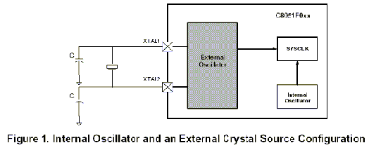
图1. 内部振荡器和外部晶体源配置
晶体振荡器和内部振荡器可以同时工作,每一个都可以根据需要被选为系统时钟源。为了减小电源电流,在使用内部振荡器时可停止晶体振荡器。在这种情况下,当从内部切换到外部振荡器时,设计者必须考虑切换系统时钟源时的起动延迟。C8051F0xx器件有一个指示外部时钟信号有效的标志位(OSCXCN寄存器中的XTLVLD位),该标志在外部振荡器稳定运行时置位。在切换到外部振荡器之前应查询该标志。注意:在外部晶体起动期间,其它操作可继续使用内部振荡器。
某些应用需要间歇的高速度和高精度(例如ADC采样和数据处理),但在其它时间可允许低速度和低精度(例如等待采样时),这时可以用到外部振荡器和RC电路的组合。在这种情况下,外部RC振荡器用于产生低频SYSCLK源,而晶体用于高频率操作。RC电路需要接到VDD(电压源)才能工作。由于在晶体处于工作状态时,这种连接可能加载晶体振荡器电路,我们将RC电路接到一个通用端口引脚(见图2),当使用RC电路时,与之连接的端口引脚被驱动到高电平(到VDD),这可以通过选择端口为“推挽”输出方式并向端口锁存器写“1”来实现。当使用晶体振荡器时,端口引脚被置于“高阻”状态,这是通过设置端口为“漏极开路”输出方式,并向端口锁存器写“1”来实现的。注意:RC电路可以利用晶体振荡器电路中已有的电容 。
RC电路振荡器的起动几乎是瞬间完成的,然而晶体振荡器的起动时间是比较可观的。因此从RC振荡器切换到外部晶体振荡器时要经过下列过程 :
a. 切换到内部振荡器 。
b. 将作为RC电路电源的端口引脚设置为漏极开路并向该端口引脚写“1”(高阻状态)。
c. 起动晶体(设置XFCN位)。
d. 等待1ms 。
e. 查询外部晶体有效位(XTLVLD --> ‘1’ )。
f. 切换到外部振荡器。
从外部晶体振荡器切换到RC振荡器的步骤如下
a. 切换到内部振荡器。
b. 关闭晶体振荡器(清除XFCN位)。
c. 驱动电源端口引脚到高电平(到VDD),通过选择端口为“推挽”输出方式并向端口锁存器写“1”来实现 。
d. 切换到外部振荡器。
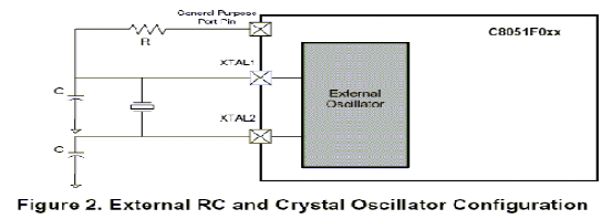 图2. 外部RC和晶体振荡器配置
5 电源电压
CMOS逻辑电路中的电流与电源电压成正比。CMOS逻辑电路的功耗与电源电压的平方成正比(见方程1)。因此降低器件的供电电压可以减小功耗,C8051Fxxx系列器件所要求的电源电压为2.7-3.6V。为了减小功耗,建议使用3.0V的稳压器而不采用3.3V的稳压器 。
CIP51处理器电源管理方式
C8051处理器有两种电源管理方式。这两种方式为等待方式和停机方式 。
6 等待方式
在等待方式下,CPU和FLASH存储器停止工作。所有外设都处于工作状态,包括内部时钟。在有中断(被允许的中断)产生或发生系统复位时CPU退出等待方式。可通过将等待方式选择位(PCON.0)设置为‘1’使CPU进入等待状态 。
当等待方式选择位被置‘1’时,一旦设置该位的那条指令执行完,CPU立即进入等待状态。有中断发生后,等待方式选择位将被清除,CPU将转入中断服务程序。从中断返回后(RETI),CPU将进入设置等待方式选择位那条指令的下一条指令。如果在等待方式下有复位条件产生,将产生正常的复位过程,CPU将从存储器地址0x0000开始执行程序 。
例如,CPU被置于等待方式,等待定时器2溢出后启动一次A/D转换。一旦转换过程结束,ADC转换结束中断将CPU从等待状态唤醒,开始处理采样值。在样本处理过程结束后,CPU又重新被置于等待方式以节省功耗,同时等待下一次中断 。
另一个例子,CPU平时处于等待方式以节省功耗,在需要时用一个外部中断信号将其“唤醒”。在收到外部中断时,CPU将退出等待方式并转到相应的中断服务向量(例如/INT0或/INT1)。
7 停机方式
C8051的停机方式用于停止CPU和振荡器。这将使所有数字外设都停止工作。在进入停机方式前必须用软件将所有的模拟外设关闭,只有内部或外部复位可以使处理器退出停机方式。实际上停机方式节省功耗是靠将SYSCLK频率降低到0 。
注意:时钟丢失检测器会产生一个内部复位(如果被允许),这个内部复位将结束停机方式。因此如果要使CPU处于停机状态的时间大于时钟丢失检测器的超时时间(100 μs),则在进入停机方式之前应禁止时钟丢失检测器。
通过将停机方式选择位置‘1’使C8051处理器处于停机方式。在复位时,CPU完成正常的复位过程并从0x0000地址开始执行程序,任何有效的复位源都可以使CPU退出停机方式。能使CPU退出停机方式的复位源是:外部复位(/RST)、时钟丢失检测器、比较器0、外部ADC转换启动信号(/CNVSTR)。
例如,CPU在不需要工作的一段时间内可以被置于停机方式以节省功耗,在需要工作时用用比较器0复位信号将其“唤醒”。
一般来说,一个低功耗的设计应采用最低的电源电压、最低的SYSCLK频率,并尽可能地使用电源管理方式,以最大限度地节省功耗。这些条件中的大多数都可以用软件实现或控制 。
8 功耗计算
在Cygnet 的C8051F00x和C8051F01x系列器件中消耗功率的两大部件是:模拟部件和数字部件。模拟部件的功耗对于所有的SYSCLK频率来说几乎是不变的;数字部件的功耗随着SYSCLK频率的不同而有较大的变化。模拟部件和数字部件的功耗加在一起构成器件的总功耗 。
本应用笔记中所介绍的器件消耗电流的计算方法适用于C8051F00x和C8051F01x(F000、01、02、05、06、10、11、12、15和16系列器件 )。
数据手册中“总体直流电气特性”一节中给出了不同条件下器件的供电电流值。电流值被分为数字部件(在三种示例频率下)和模拟部件两部分。所给出的模拟电流值是所有模拟外设都工作时的数值。每个模拟外设的供电电流可以在数据手册中与外设相关的章节中查到 。
9 内部和外部振荡器比较
除了使用较低的SYSCLK频率之外,设计者还可以通过合理地选择时钟源达到减小功耗的目的。内部振荡器消耗数字电源电流的典型值为200 μA,用于驱动外部振荡器的电流是变化的。对于一个外部振荡源(例如一个晶体),驱动电流(由模拟电源提供)用软件通过配置外部振荡器控制寄存器(OSCXCN)的XFCN位来设置。在驱动电流较大时,用户可以使用内部振荡器以节省功耗,但是在最低的XFCN设置下,外部振荡器使用不到1μA的电流,小于内部振荡器所使用的电流。下面列出了几个典型测量电流值。这些测量值对于不同的器件可能不一样。驱动电平应保持最低以节省功耗,但又应足够高以使外部振荡器能够起振。下表列出了电流与外部振荡器频率控制位设置的关系。
10 数字外设
对于粗略的计算,一个经验公式是假设1mA/MHz的工作电流+1mA,如果模拟部件(ADC、比较器、DAC、VREF等被允许)。这个经验公式假定使用3.6V的电源电压。较低的电源电压将使功耗降低。在2.7V经验公式为 0.5mA/MHz(在正常方式)。下表列出了用于估算电源电流的经验数据 。
数字电流消耗典型值
| 电源方式 | VDD=2.7V | VDD=3.6V |
| 正常 | 0.5mA/MHz | 1.0mA/MHz |
| 等待 | 0.33mA/MHz | 0.65mA/MHz |
注意:数字电源电流与使用多少个数字外设无关 ,电源电流与SYSCLK的频率及电源 电压成正比。
11 模拟外设
每个模拟外设的供电电流值都在数据表中关于这个外设的部分给出(通常在该部分的最后)。建议禁止所有不用的外设部件以降低功耗。为方便起见,将C8051F00x和C8051F01x模拟外设的供电电流值列于下表:
C8051F0xx模拟外设供电电流
| 模拟外设 | 典型电流值μA |
| VDD监视器 总处于允许状态 | 8VDD=2.7V 15VDD=3.6V |
| ADC | 450 |
| VREF内部 | 50带隙基准和驱动器 |
| 温度传感器 | 10 |
| 比较器 | 1.5每个 |
| DAC | 110每个 |
| 内部振荡器 使用数字电源 | 200 |
注意:模拟功耗与SYSCLK频率相对无关。
12 总电流计算
当所需要的SYSCLK频率、电源电压及外设部件都已经确定后,可以估算总的电源电流。所使用的模拟外设电流(将每个被允许的模拟外设的电流加在一起)加上所使用的数字电流(在给定频率、电源方式和电源电压下计算)就得到总的电源电流。如果所有的模拟外设都被允许,则所用模拟电流大约为1mA 。
13 计算举例
下面是电源电流计算的几个例子。每个应用在不同的时间,可以使用不同的电源方式、SYSCLK频率和外设部件。因此,功率管理指标需要几种不同的电源电流计算。数字部件和模拟部件所使用的电流分别计算然后加到一起得到总电流 。
例1
在一个VDD=3.6V的系统中使用C8051F000器件。ADC对一个参数采样,将样本处理后经DAC输出。由于在该应用中需要进行采样和处理,选择内部振荡器提供16MHz的SYSCLK频率 。
模拟部件:
| 外设 | 供电电流μA |
| ADC | 450 |
| VREF内部 | 50 |
| 内部振荡器 | 200 |
| 一个DAC | 110 |
| VDD监视器 | 15 |
| 总模拟电流 | 825 |
| | |
数字部件:在正常方式工作频率为16 MHz;1mA/MHz * 16 MHz = 16mA
总电流:825μA(模拟)+ 16mA(数字)= 16.8mA
例2
假设我们仍然估算例1中同一个应用的电源电流。如果采样处理是一个猝发操作(即间歇性地需要采样和转换),我们可以选择平时将CIP-51置于等待方式,经过一个规定的时间间隔后,再用一个定时器将其“唤醒”。在这种情况下,可以通过计算平均电流来估算功率需求。器件将在正常方式(用于采样和数据转换)和等待方式(在两个采样处理操作之间)之间切换。在正常方式和等待方式之间切换的周期等于采样速率。这就允许我们在计算了等待方式的电源电流之后计算平均电源电流。
模拟部件:
在两次采样处理和输出之间,器件处于等待方式,模拟外设被禁止。这种情况下模拟电流消耗为 :
VDD监视器 = 15μA
数字部件:
在等待方式,工作频率为16 MHz
0.65mA/MHz * 16 MHz = 10.4mA
总电流
在大多数应用中,模拟部件的功耗可以被忽略,这样一来总电流就是数字部件的电流 :
50 μA(模拟)+ 10.4mA(数字)= 10.4mA
注意,我们已经计算了等待方式下的电源电流和正常方式下的电源电流(在例1中)。我们还必须计算在每种方式下所消耗的时间,以计算所用器件的平均电流 。
假设ADC工作在低功耗跟踪方式,使用最大的2MHz SAR转换时钟(ADC设置为:SAR时钟 = SYSCLK/8),我们需要10kHz的采样速率。图3中的电源周期为 1/10,000(采样速率)= 100 μs 。
处在正常方式下的时间是ADC跟踪/转换时间和将样本保存到存储器的时间。在低功耗跟踪方式,需要3个SAR时钟用于跟踪和16个SAR时钟用于转换。这19个SAR时钟在频率为2MHz时需要9.5 μs。存储采样值需要两个系统时钟周期即0.125 μs。为了进入正常方式,要执行一条mov指令,需三个SYSCLK周期,即0.188μs。这样在正常方式下的总时间为 9.5 μs + 0.125 μs+ 0.188 μs = 9.8 μs 。
因为ADC的采样周期是100 μs,所以在电源周期中等待方式所占的时间为 100 μs – 9.8 μs(正常方式下的时间)= 90.2 μs。对图3曲线下方的区域在一个周期(100 μs)内积分,然后除以周期值,得到平均电源电流为 11 mA 。16.8mA\10.4mA等待方式采样周期时间数据采样和转换正常方式电流。
例3
如果在器件处于等待方式(在例2中)时使用一个外部振荡器,使振荡器的频率降低到32kHz,可以进一步降低功耗。这时所用的电流是:
将外部振荡器控制位设置为XFCN = 000。这样将使用0.6 μA的模拟电流 。
(0.65mA * 0.032MHz) + 0.6 μA = 21 μA
这与例2中16MHz下的等待方式有惊人的差别,只是通过简单地降低振荡器频率。
继续进行列2中(在正常方式有6个附加的SYSCLK周期用于降低振荡器频率)的平均电流计算得到的平均电流为1.7mA 。
例4
在这个应用中,用C8051F000的ADC对一个参数采样并将采样值保存到存储器中,需要对采样精确定时。为了满足更精确的定时要求,SYSCLK由一个外部18.432 MHz晶体振荡器提供。为了节省功耗,设计者决定使用3.0V的电源电压。定时器2用于对ADC采样间隔定时 。
模拟部件:
| 外设 | 供电电流μA |
| ADC | 450 |
| 外部振荡器驱动器 XFCN=111 | 2900 |
| VDD监视器 | 15 |
| 总模拟电流 | 3361 |
数字部件:
在正常方式,工作频率为18.432MHz;0.8mA/MHz * 18.432 MHz = 14.7mA
总电流:3.4mA模拟+ 14.7mA数字= 18.1mA
例4 在等待方式时的电流
如果采样操作是猝发式的在不需要采样的时间段内将器件置于等待方式并禁止ADC不需CIP-51操作数字外设继续工作将节省功耗在等待方式所消耗的数字电流仅为0.6mA/MHz如果没有ADC转换在18.432 MHz下电流消耗= 11.1mA
计算一个采样周期内的平均电源电流与例2类似假设10 kHz的采样频率和低功耗跟踪方式平均电流的估算值为 11.9mA.
致 谢
设计是我们的大学学习生活的最后一项学习任务,是对我们大学四年学习的综合考核。为期两个多月的设计过程中,我不仅较为系统的复习了以前学的知识,而且又学习了许多新知识,使我的知识更加系统化,更加完善。同时,也提高了独立分析问题、解决问题的能力。相信设计一定会为我们在不久的将来踏上工作岗位打下了良好的实践基础。
本次设计能够顺利地完成,首先要感谢我的指导老师王锦教授。王教授严谨的治学态度,深厚的学术造诣以及忘我的工作精神给我留下了深刻的印象。王教授的严格要求和孜孜不倦的教导是我完成这次设计的重要保证,她给予了我很大的帮助和支持,在课题研究期间,王教授提供了很多指导性的意见,对存在的问题给予细心的分析并提出许多宝贵的意见,使我受益匪浅;同时为我们提供了良好的设计场所和试验条件。在此谨向导师表示衷心的感谢!当然,我也要感谢给予我帮助和支持的朋友们,感谢在编程和电路调试过程中给我提供帮助的王博同学,感谢电子工程系的老师为我们做设计提供的各方面的帮助!
同时,我要感谢我的母校——天津工程师范学院。大学四年,这里留下了我们许多美好的回忆。特别是在我即将踏上工作岗位的同时,给了我这样一个锻炼、学习的机会,使我加深了对以前知识的理解,拓宽了知识面,也提高了我对所学知识的综合的应用能力。我忠心地祝愿母校的未来更美好!