10 ANALOG - TO - DIGTAL CONVERTERS WITH SERIAL CONTROL
引脚图:

TLC 1549 可有六种工作时序 ,主要是考虑硬件SPI 接口的速度,因为硬件实现的SPI必须按字节读写,而1549是10位AD转换器,所以要读取转换结果必须按两字节既16位操作,故出现了那么多工作模式。当采用软件模拟SPI时序时,就不必考虑区分这6种模式了。
采用GPIO产生控制时序通常采用10时钟周期模式,

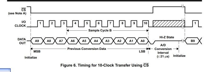
10 时钟转换 使用CS

10时钟不适用 CS
由上图所示、当CS 下降沿和第一个周期的下降沿读取高两位,其余8个周期用于读取低8位。从第3个周期下降沿到第10个周期下降沿为片内采样周期,然后从第10个周期下降沿开始后的21us 为转换周期,片选信号CS 通常采用转换期间无效模式,既在转换过程中把 拉高CS (Figure 6).这是考虑到芯片的功耗问题,因为使能芯片比禁止芯片功耗要多出许多,这一点可直接从1549的datasheet中看出。
从控制时序图中可以看出,一个完整AD 转换周期包括读取、采样和量化(转化)三个过程周期,而且读取周期和采样周期部分是重叠的,另外1549转换的一个重要特点是读取的数据是上次启动AD转换的结果,这就带来一个问题,1549上电后第一次转换如何处理?
显然芯片上电复位后,输出寄存器内容并非某次AD转换结果,可能是一个随机数或某个常数,若直接进行转换,首次读出的数据当然是错误的,不过可以采用初始化的方法确保首次读出的数据为第一次启动AD转换的结果,具体方法是,在上电后首次执行一个初始化函数ADCClnit(),在函数中输出10个周期脉冲,在第10个脉冲的下降沿,AD转换被启动,然后等待21us ,最后才进入正常的AD转换程序,以后的读取的数据就可以确定是AD转换的真实值了。
在实际数据采集过程中,
description
The TL1549,TLC1591,and TLC1549M are 10-bit,switched-capacitor,successive-approximation(连续近似的)analog-to-digital converters.these devices have two digital inputs and 3-state output [chip select (cs低电平有效) ,input-output clock (I/O clock),and data output (DATA OUT)] that provide a three-wire interface to the serial port of a host processor.
The sample-and-hold function is automatic . The converter incorported in these devices features differentil high-impedance reference inputs that facilitate ratiometric conversion,scaling(比例),and isolation(绝缘) of analog ciruitry from logic and supply noise.a switched-capacitor (转换电容器) design allows low-error converson over th full operating free-air temperature range.
The TLC1549C is characterized for operation from 0度 to 70度 。The TLC15491 is characterized for operation from -40 度 to 85度. The TLC 1549M is characterized for operation over the full military temperature range of -55度 to 125度。
detailed description
with chip select (cs) inactive (high),I/O clock is initially disabled and DATA OUT is in the high-impedance state. When the serial interface takes cs active (low ),the cnversion sequence begins with the enabling of I/O clock and the removal of DATA OUT from the high-impedance state.the serial interface then provides the I/O clock sequence to I/O clock and receives the previous conversion result fro DATA OUT .I/O clock receives an input sequence that is between 10 and 16 clock long from the host serial interface .the first ten I/O clocks provide the control timing for sampling the analog input.
there are six basic serial interface timign modes that can be used with the TLC1549. These modes are determined by the speed of I/O clock and the operation of cs shown in Table .these modes are(1) a fast mode with a 10 clock transfer and cs inactive (high ) between transfers,(2)a fast mode with a 10-clock transfer and cs active (low) continuously,(3) a fast mode with an 11-to 16 clock transfer and cs inactive (high) between transfes ,(4) a fast mode with a 16-bit transfer and cs active (low) continuously,(5) a slow mode with an 11 - to 16 -clock transfer and cs inactive (high)between transfers,and(6)a slow mode with a 16 -clock transfer and cs active(low)continuously.
The MSB of the previous conversion appears on DATA OUT on the falling edge of cs in mode 1,mode 3,and mode 5,withi 21 us from the falling edge of the tenth I/O clock in mode 2 and mode 4,and following the sixteenth clock falling eddge in mode 6.the remaining nine bits are shifted out on the next nine falling edges of I/O clock .Ten bits of data are transmitted to the host serial intrface through DATA OUT.The number of serial clock pulses used also depends on the mode of operation,but a minimum of ten clock pulses is required for conversion o begin.on the tenth clock falling edge,the internal logic takes DATA OUT low to ensure that the remaining bit values are zero if the I/O clock transfer is more than ten clocks long.